Methods and techniques for PCB board dissection
PCB board dissection is an important part of PCB design. However, since it involves sandpaper grinding (a harmful type of work) and line drawing (a simple repetitive labor), many designers are reluctant to do this work. Even many designers think that PCB board dissection is not a technical job, and junior designers can do this job with a little training. This concept is somewhat universal, but like many jobs, there are still some skills in PCB board dissection. If designers master these skills, they can save a lot of time and greatly reduce the workload. Let’s talk about this knowledge in detail below.
Concept of PCB board dissection
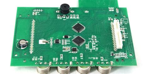
PCB board dissection refers to the process of obtaining the schematic diagram and board diagram (PCB diagram) based on the original PCB board. Its purpose is to carry out later development. Later development includes installing components, deep testing, modifying circuits, etc. Because it does not belong to the scope of PCB board dissection and is related to it, it is only introduced and no longer detailed.
Process of PCB board dissection
- Remove the components on the original board.
- Scan the original board to obtain the graphic file.
- Grind off the surface layer to get the middle layer.
- Scan the middle layer to get the graphic file.
- Repeat steps 2-4 until all layers are processed.
- Use special software to convert the graphic file into an electrical relationship file—PCB diagram. If there is suitable software, the designer only needs to trace the graphic once.
- Check and verify to complete the design.
PCB board dissection skills
PCB board dissection, especially multi-layer PCB board dissection, is a time-consuming and laborious task, which includes a lot of repetitive labor. Designers must have enough patience and care, otherwise it is very easy to make mistakes. The key to doing a good job of dissecting PCB board design is to use suitable software instead of manual repetitive work, which is time-saving and accurate.
1.A scanner must be used during the dissection process.
Many designers are accustomed to drawing lines directly on PCB design systems such as PROTEL, PADSOR or CAD. This habit is very bad. The scanned graphic file is both the basis for conversion into PCB files and the basis for later inspection. Using a scanner can greatly reduce the difficulty and intensity of labor. It is no exaggeration to say that if the scanner can be fully utilized, even people without design experience can complete the PCB board profiling work.
2.Single-direction grinding.
In order to pursue speed, some designers choose two-way grinding (that is, grinding the board layer from the front and back surfaces to the middle layer). In fact, this is very wrong. Because the two-way grinding board is very easy to wear through, causing damage to other layers, the result can be imagined. The outer layer of the PCB board is the hardest due to the process and copper foil, pads, etc., and the middle layer is the softest. Therefore, the problem is more serious when it comes to the middle layer, and it is often impossible to grind. In addition, the PCB boards produced by various manufacturers have different materials, hardness, and elasticity, which makes it difficult to grind accurately.
3.Choose excellent conversion software.
Converting the scanned graphic file to a PCB file is the key to the entire work. With a good conversion file. Designers only need to “copy the cat and draw the tiger” and trace the graphic once to complete the work. EDA2000 is recommended here, which is really convenient.