Methods for Disconnecting Surface Traces on PCBs: A Comprehensive Guide
Printed Circuit Boards (PCBs) are the backbone of modern electronics, providing the necessary electrical connections between components. However, during prototyping, debugging, or repair, engineers often need to disconnect surface traces to isolate circuits, fix errors, or modify designs. This article explores various methods for disconnecting PCB surface traces, their advantages, disadvantages, and best practices.
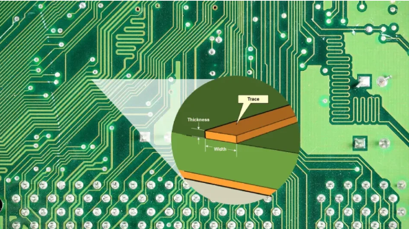
1. Introduction to PCB Trace Disconnection
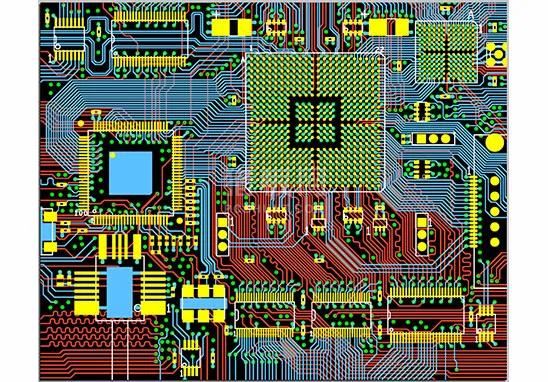
PCB traces are conductive pathways, typically made of copper, that connect different components on a board. Disconnecting a trace may be necessary for:
- Debugging and Testing: Isolating a section of a circuit to identify faults.
- Design Modifications: Altering connections without redesigning the entire PCB.
- Repair Work: Fixing short circuits or unwanted connections.
Several techniques can be used to break a trace, ranging from manual cutting to advanced laser methods.
2. Manual Cutting with a Knife or Scalpel
Procedure:
- Use a sharp precision knife (e.g., X-Acto knife) or scalpel.
- Carefully scratch along the trace multiple times until the copper is fully severed.
- Verify the disconnection using a multimeter.
Advantages:
- Low cost and requires no special tools.
- Quick for simple modifications.
Disadvantages:
- Risk of damaging adjacent traces or the PCB substrate.
- Inconsistent cuts may leave residual conductive material.
Best Practices:
- Work under magnification for precision.
- Use multiple light passes rather than a single deep cut.
3. Using a Rotary Tool (Dremel) or PCB Cutter
Procedure:
- Use a fine grinding bit or a specialized PCB cutting wheel.
- Gently grind away the copper trace until an open circuit is confirmed.
Advantages:
- Faster than manual cutting for thicker traces.
- More consistent results with proper tools.
Disadvantages:
- Risk of excessive material removal.
- Generates copper dust, which can cause short circuits if not cleaned properly.
Best Practices:
- Use low speed to avoid overheating.
- Clean the area with isopropyl alcohol afterward.
4. Abrasive Methods (Sandpaper or Fiberglass Pen)
Procedure:
- Rub fine-grit sandpaper or a fiberglass pen over the trace until the copper is removed.
- Check continuity to ensure complete disconnection.
Advantages:
- No risk of deep cuts damaging the PCB.
- Useful for thin traces.
Disadvantages:
- Time-consuming for wide traces.
- May affect nearby components or solder mask.
Best Practices:
- Use masking tape to protect surrounding areas.
5. Soldering Iron and Solder Wick (For Thin Traces)
Procedure:
- Apply flux to the trace.
- Heat the trace with a soldering iron while using solder wick to remove copper.
- Repeat until the trace is fully disconnected.
Advantages:
- Precise for very thin traces.
- Minimal mechanical stress on the PCB.
Disadvantages:
- Risk of overheating and damaging the substrate.
- Not suitable for thick copper layers.
Best Practices:
- Use a temperature-controlled soldering iron.
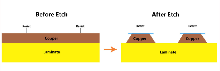
6. Chemical Etching (For Selective Trace Removal)
Procedure:
- Apply an etch-resistant mask (e.g., tape or resist pen) to protect unaffected areas.
- Use ferric chloride or ammonium persulfate to dissolve the exposed copper.
- Rinse and clean the PCB thoroughly.
Advantages:
- Precise for complex modifications.
- No mechanical stress on the PCB.
Disadvantages:
- Requires hazardous chemicals.
- Over-etching can weaken nearby traces.
Best Practices:
- Neutralize and dispose of chemicals properly.
7. Laser Ablation (High-Precision Industrial Method)
Procedure:
- Use a UV or CO₂ laser to vaporize the copper trace.
- Commonly used in PCB manufacturing and repair facilities.
Advantages:
- Extremely precise, with micron-level accuracy.
- No physical contact prevents mechanical damage.
Disadvantages:
- Expensive equipment.
- Requires specialized training.
Best Practices:
- Optimize laser power and speed settings.
8. Micro-Drilling (For Complete Trace Isolation)
Procedure:
- Use a high-speed micro drill (0.3–1.0 mm) to create a small hole through the trace.
- Ensures complete electrical separation.
Advantages:
- Guarantees a clean break.
- Useful for multilayer PCBs.
Disadvantages:
- May weaken the PCB structurally.
- Requires precise alignment.
Best Practices:
- Use a drill press for stability.
9. Comparison of Methods
| Method | Precision | Cost | Risk of Damage | Best For |
|---|---|---|---|---|
| Manual Cutting | Medium | Low | High | Quick fixes |
| Rotary Tool | Medium | Low | Medium | Thicker traces |
| Abrasive Methods | Low | Low | Low | Thin traces |
| Soldering Iron | High | Low | Medium | SMD traces |
| Chemical Etching | High | Medium | Medium | Complex cuts |
| Laser Ablation | Very High | High | Low | Industrial use |
| Micro-Drilling | High | Medium | Medium | Multilayer PCBs |
10. Conclusion
Choosing the right method for disconnecting PCB traces depends on factors like precision requirements, available tools, and the PCB’s complexity. For hobbyists, manual cutting or a rotary tool may suffice, while professionals might prefer laser ablation or micro-drilling. Always verify the disconnection with a multimeter and follow best practices to avoid unintended damage.
By understanding these techniques, engineers and technicians can efficiently modify and repair PCBs, ensuring optimal performance in electronic systems.