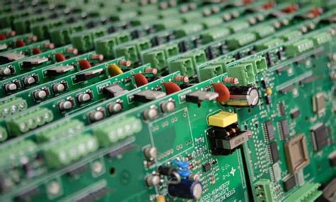
Methods for making circuit boards under amateur conditions
Circuit boards are the carriers of electronic circuits. Any circuit design needs to be installed on a circuit board to realize its function. Processing circuit boards is the most headache for amateur electronics enthusiasts. It is often the case that the circuit is designed in half a day, but it takes several days to process the circuit board. Even some good circuit design ideas are abandoned because the processing of circuit boards takes too much time and cannot be realized. How to process experimental circuit boards simply, quickly, at low cost and with high quality is a topic worth studying. Now there are many new and good methods, such as thermal transfer method, pre-coated photosensitive copper plate production method, hot melt plastic film method, etc.
Regular production of printed circuit boards is naturally related to printing.
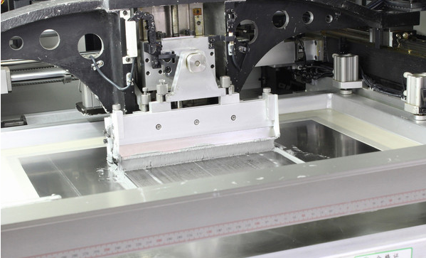
The screen printing process is usually used. The basic process is as follows: Design layout → Tracing → Board exposure (making printing base) → Printing → Chemical corrosion → Cleaning and surface treatment → Printing soldering, logo, solder mask and other layers → Cutting, punching and other mechanical processing → Finished circuit board
Under amateur conditions, the process of “printing soldering, marking, solder mask and other layers” can be omitted, and the difficulty lies in the plate making and printing links. Since only a small number (one or several) of circuit boards need to be made, it is obviously not economical to use formal plate making and printing processes, so there are various non-printing or sub-printing production methods.
1.Engraving method:
This method is the most direct. Use carbon paper to copy the designed copper foil pattern to the copper foil surface of the copper clad board, use a special engraving tool made of a hacksaw blade to directly carve along the edge of the copper foil pattern on the copper clad board, try to cut as deep as possible, and then tear off the unnecessary copper foil outside the pattern, and then punch the component jack. The key to this method is: the carving force must be enough; tear off the excess copper foil from the edge of the board. When the operation is good, it can be gradually torn off in pieces, and nail clippers can be used to complete this step. Some small circuit experimental boards are suitable for production using this method.
2.Manual drawing method:
It is to use a pen to directly draw the printed pattern on the copper clad board, and then perform chemical etching and other steps. This method seems simple, but it is not easy to operate in practice! Nowadays, electronic components are small in size, the pin spacing is even smaller (millimeter level), the copper foil routing is also very small, and the lines drawn are difficult to modify. To draw such a board well depends entirely on your pen skills. Experience is: the selection of “pigment” and brush is very important. I have tried using anhydrous alcohol and rosin. The effect depends on the degree of carefulness and the good drawing.
3.Posting method:
Electronic stores sell a kind of “standard pre-cut symbols and tapes”. The common specifications of pre-cut symbols are D373 (0D-2.79, ID-0.79), D266 (0D-2.00, ID-0.80), D237 (OD-3.50, ID-1.50) and other types. It is best to buy paper-based materials (black), and try not to use plastic-based (red) materials. The common specifications of tapes are 0.3, 0.9, 1.8, 2.3, 3.7 and other types. The unit is millimeter. According to the circuit design layout, you can choose the corresponding symbols and tapes and paste them on the copper foil surface of the copper-clad plate. Use a softer hammer, such as smooth rubber, plastic, etc. to hit the sticker to make it fully adhere to the copper foil. Focus on the turning points and overlaps of the lines. When it is cold, it is best to use a heater to warm the surface to enhance the adhesion effect. After posting, you can proceed with the corrosion process.
4.Mimeograph method:
Put the wax paper on the steel plate, use a pen to carve the circuit diagram on the wax paper at a 1:1 ratio, and cut the circuit diagram carved on the wax paper according to the size of the circuit board, and put the cut wax paper on the printed copper-clad plate. Take a small amount of paint and talcum powder to make a suitable printing material, dip the printing material with a brush, and evenly apply it to the wax paper. Repeat several times, and the printed board can be printed with the circuit. This type of stereotype can be used repeatedly and is suitable for small batch production. Tip: Using a photoelectric copier, you can automatically carve a 1:1 size wax paper according to the design drawing.
5.Hot melt plastic film plate making method: I have only heard of this method, but I have not found the specific production method. If you have information, please continue. 6. Use pre-coated photosensitive copper-clad board: This should be very familiar to everyone. It is a special copper-clad board. The surface of its copper-platinum layer is pre-coated with a layer of photosensitive material, so it is called “pre-coated photosensitive copper-clad board”, also called “photosensitive board”. The production method is as follows:
① Production of single-sided board: Print out 1:1 black and white 720dpi drawings (component surface) with special inkjet paper for PCB drawings drawn by computer. It is also OK to output drawings with laser printer. Take a photosensitive board of the same size as the drawing and tear off the protective film. Press the drawing and the photosensitive PCB board with a glass plate or a plastic transparent plate, and expose them to the sun for 5-10 minutes. Use the attached developer with a ratio of 1:20 to water for development. When the exposed part (unnecessary copper foil) is completely exposed, rinse it with water and then use ferric chloride for corrosion. After proficiency in operation, you can make a trace with an accuracy of 0.1mm!
② Production of double-sided circuit boards: The steps refer to single-sided boards. The main thing about double-sided boards is that the positioning of both sides must be accurate. Both sides can be exposed separately, but the time must be consistent. When one side is exposed, the other side must be protected with black paper.
This method is the simplest and most practical method in principle, but the “pre-coated photosensitive copper-clad board” on the market is relatively expensive and difficult to buy.
7.Thermal transfer method:
Use a laser printer to print the designed PCB copper-platinum graphics on thermal transfer paper, and then press the thermal transfer paper against the copper-platinum surface of the copper-clad board. Heat it at an appropriate temperature, and the graphics originally printed on the transfer paper (actually carbon powder) will melt due to the heat and transfer to the copper-platinum surface to form a corrosion protection layer. This method is simpler than the conventional plate-making and printing method, and most circuits are now designed using computer CAD, and laser printers are also quite popular. This process is relatively easy to implement.
You can choose the method of making PCB boards according to your actual situation. Although it cannot be compared with professional production, it is suitable for amateur production.