Methods to Eliminate Crosstalk in PCB Design
Abstract
Crosstalk is a common issue in high-speed printed circuit board (PCB) designs, where unwanted electromagnetic coupling between adjacent signal traces degrades signal integrity. This paper explores various techniques to minimize crosstalk in PCB layouts, including proper trace spacing, grounding strategies, differential signaling, and impedance control. By implementing these methods, designers can enhance signal quality, reduce electromagnetic interference (EMI), and improve overall system performance.
1. Introduction
Crosstalk occurs when signals from one trace interfere with another due to capacitive (electric field) or inductive (magnetic field) coupling. In high-speed digital and RF circuits, crosstalk can lead to data corruption, timing errors, and increased EMI. To mitigate these effects, PCB designers must adopt strategies that minimize unwanted signal coupling while maintaining signal integrity.
This paper discusses key approaches to reducing crosstalk, including:
- Proper trace routing and spacing
- Ground plane utilization
- Differential pair routing
- Impedance matching
- Shielding techniques
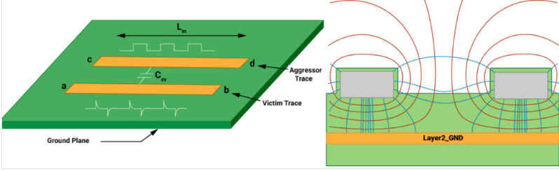
2. Understanding Crosstalk Mechanisms
Crosstalk manifests in two forms:
- Near-End Crosstalk (NEXT): Interference measured at the source end of the victim trace.
- Far-End Crosstalk (FEXT): Interference measured at the far end of the victim trace.
The primary causes of crosstalk include:
- High-frequency signal transitions
- Long parallel trace runs
- Inadequate spacing between traces
- Poor return path design
3. Techniques to Minimize Crosstalk in PCB Design
3.1. Trace Spacing and the 3W Rule
One of the simplest ways to reduce crosstalk is by increasing the distance between signal traces. The 3W Rule suggests that the spacing between adjacent traces should be at least three times the width of the trace (W). For example, if a trace is 6 mils wide, the minimum spacing should be 18 mils.
- Advantages:
- Reduces capacitive coupling
- Easy to implement in low-density designs
- Limitations:
- May not be sufficient for very high-speed signals (>1 GHz)
- Increases PCB size in dense layouts
3.2. Ground Plane and Return Path Optimization
A solid ground plane beneath signal layers helps minimize crosstalk by providing a low-impedance return path. Key considerations include:
- Avoiding splits in the ground plane under high-speed traces
- Using stitching vias to connect ground planes in multilayer PCBs
- Ensuring a continuous return path for high-frequency signals
3.3. Differential Pair Routing
Differential signaling (e.g., USB, PCIe, LVDS) inherently reduces crosstalk because:
- The two traces carry equal and opposite signals, canceling out electromagnetic interference.
- Crosstalk affects both traces similarly, maintaining signal integrity.
Best practices for differential pairs:
- Maintain consistent spacing (controlled impedance)
- Route traces symmetrically to avoid skew
- Avoid abrupt bends (use 45° or curved traces)
3.4. Impedance Control and Termination
Proper impedance matching prevents signal reflections, which can exacerbate crosstalk. Techniques include:
- Using microstrip or stripline transmission line structures
- Adding termination resistors to match trace impedance
- Avoiding impedance discontinuities (e.g., vias, stubs)
3.5. Shielding and Guard Traces
For extremely sensitive signals, additional shielding techniques can be applied:
- Guard Traces: Adding grounded traces between high-speed signals to block coupling.
- Shielded Cables: Using coaxial or twisted-pair cables for off-board connections.
- Faraday Cage: Enclosing critical components in a conductive shield.
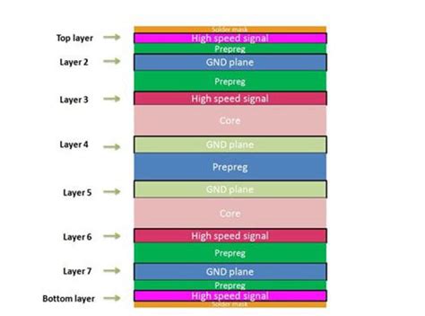
3.6. Layer Stackup Optimization
A well-designed PCB stackup can significantly reduce crosstalk:
- Route high-speed signals on inner layers between ground planes.
- Separate noisy digital and sensitive analog signals into different layers.
- Use buried vias to minimize stub effects in high-frequency designs.
3.7. Reducing Parallel Trace Lengths
Long parallel traces increase inductive coupling. Mitigation strategies include:
- Routing critical signals orthogonally on adjacent layers
- Using serpentine routing to minimize parallel sections
- Keeping high-speed traces short and direct
3.8. Simulation and Validation
Before fabrication, crosstalk effects should be simulated using tools such as:
- SPICE-based simulators (e.g., LTspice, PSpice)
- 3D EM field solvers (e.g., Ansys HFSS, CST Studio)
- Signal integrity analysis (e.g., HyperLynx, Sigrity)

4. Practical Case Study: Reducing Crosstalk in a High-Speed DDR4 Design
A real-world example involves a DDR4 memory interface where crosstalk was causing timing violations. The following changes were implemented:
- Increased trace spacing from 5 mil to 12 mil (applying the 3W rule).
- Added guard traces between data lines.
- Optimized the ground plane to eliminate splits.
- Used differential routing for clock signals.
Results:
- Crosstalk-induced jitter reduced by 40%.
- Signal-to-noise ratio (SNR) improved by 15 dB.
5. Conclusion
Crosstalk is a critical challenge in modern PCB design, especially with increasing signal speeds and density. By applying techniques such as proper trace spacing, ground plane optimization, differential signaling, and impedance control, designers can significantly reduce crosstalk and enhance signal integrity. Simulation and validation further ensure that the design meets performance requirements before manufacturing.
Future trends in crosstalk mitigation may involve AI-assisted PCB routing, advanced materials with lower dielectric loss, and 3D-printed embedded shielding structures.