Mfs flexible pcb
Advantages Of MFS Flexible PCB In Modern Electronics
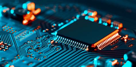
MFS flexible printed circuit boards (PCBs) have emerged as a pivotal innovation in the realm of modern electronics, offering a multitude of advantages that cater to the evolving demands of contemporary technology. As electronic devices become increasingly compact and sophisticated, the need for components that can accommodate these changes has become paramount. MFS flexible PCBs, with their unique properties, provide a solution that not only meets but often exceeds these requirements.
One of the primary advantages of MFS flexible PCBs is their remarkable flexibility, which allows them to be bent, folded, or twisted without compromising their functionality.
This characteristic is particularly beneficial in applications where space is at a premium, such as in smartphones, wearable devices, and medical equipment. By enabling the design of more compact and lightweight devices, MFS flexible PCBs contribute to the miniaturization trend that is prevalent in the electronics industry today. Furthermore, their ability to conform to various shapes and contours makes them ideal for use in complex assemblies where traditional rigid PCBs would be impractical.
In addition to their physical flexibility, MFS flexible PCBs offer enhanced reliability and durability.
The materials used in their construction are typically resistant to environmental stressors such as heat, moisture, and vibration, which can be detrimental to electronic components. This resilience ensures that devices incorporating MFS flexible PCBs maintain their performance over extended periods, even in challenging conditions. Consequently, they are well-suited for use in automotive, aerospace, and industrial applications, where reliability is of utmost importance.
Moreover, MFS flexible PCBs facilitate improved electrical performance due to their ability to reduce the number of interconnects required in a circuit.
By minimizing the need for connectors and solder joints, which are potential points of failure, these PCBs enhance signal integrity and reduce the likelihood of electrical faults. This advantage is particularly significant in high-frequency applications, where maintaining signal quality is critical. As a result, MFS flexible PCBs are increasingly being adopted in telecommunications and data transmission systems, where they contribute to the efficient and reliable operation of these networks.
Another noteworthy benefit of MFS flexible PCBs is their potential for cost savings in both manufacturing and assembly processes.
The reduction in the number of components and interconnects not only simplifies the design but also decreases the complexity of the assembly process. This simplification can lead to lower production costs and shorter lead times, making MFS flexible PCBs an economically attractive option for manufacturers. Additionally, their lightweight nature can result in reduced shipping costs, further enhancing their cost-effectiveness.
In conclusion, the advantages of MFS flexible PCBs in modern electronics are manifold, encompassing flexibility, reliability, improved electrical performance, and cost savings. As the demand for more compact, efficient, and reliable electronic devices continues to grow, the role of MFS flexible PCBs is likely to become even more significant. By addressing the challenges posed by traditional rigid PCBs and offering a versatile solution that meets the needs of various industries, MFS flexible PCBs are poised to play a crucial role in the future of electronic design and manufacturing.
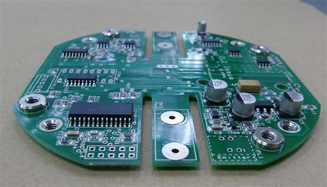
Design Considerations For MFS Flexible PCB Applications
When designing MFS (Micro Flexible Systems) flexible PCBs, several critical considerations must be taken into account to ensure optimal performance and reliability. These considerations are essential due to the unique characteristics and applications of flexible PCBs, which differ significantly from their rigid counterparts. Understanding these differences and the specific requirements of MFS flexible PCBs is crucial for engineers and designers aiming to leverage their advantages in various applications.
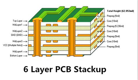
To begin with, material selection is a fundamental aspect of designing MFS flexible PCBs.
The choice of substrate material can significantly impact the flexibility, durability, and thermal performance of the PCB. Polyimide is commonly used due to its excellent thermal stability and flexibility, making it suitable for applications that require bending and folding. However, depending on the specific application requirements, other materials such as polyester or liquid crystal polymer may also be considered. The selected material must align with the environmental conditions the PCB will encounter, including temperature fluctuations and exposure to chemicals.
In addition to material selection, the design of the circuit layout is another critical consideration.
The layout must accommodate the mechanical stresses that the flexible PCB will experience during operation. This involves strategically placing components and routing traces to minimize stress concentrations and potential failure points. Designers often employ techniques such as curved traces and staggered vias to enhance the mechanical resilience of the PCB. Furthermore, the use of reinforcement materials, such as stiffeners, can provide additional support in areas that require extra rigidity, ensuring that the PCB maintains its integrity under mechanical stress.
Moreover, the thickness of the flexible PCB is a vital parameter that influences its flexibility and performance.
Thinner PCBs offer greater flexibility, which is advantageous in applications where space constraints are a concern. However, a balance must be struck between flexibility and mechanical strength, as excessively thin PCBs may be prone to damage. Therefore, designers must carefully evaluate the application’s requirements to determine the optimal thickness that provides the necessary flexibility without compromising durability.
Transitioning to the electrical considerations, signal integrity is a paramount concern in MFS flexible PCB design.
The flexible nature of these PCBs can introduce challenges related to impedance control and electromagnetic interference. To address these issues, designers must pay close attention to trace width, spacing, and the use of ground planes. Implementing controlled impedance designs and incorporating shielding techniques can help mitigate signal integrity issues, ensuring reliable performance in high-frequency applications.
Furthermore, thermal management is another crucial aspect that cannot be overlooked.
Flexible PCBs are often used in compact and densely packed electronic devices, where heat dissipation can be a challenge. Effective thermal management strategies, such as the use of thermal vias and heat spreaders, are essential to prevent overheating and ensure the longevity of the PCB. Additionally, selecting materials with good thermal conductivity can aid in dissipating heat more efficiently.
In conclusion, designing MFS flexible PCBs requires a comprehensive understanding of both mechanical and electrical considerations. By carefully selecting materials, optimizing circuit layouts, and addressing signal integrity and thermal management challenges, designers can create flexible PCBs that meet the demanding requirements of modern electronic applications. As technology continues to advance, the importance of these design considerations will only grow, underscoring the need for meticulous planning and execution in the development of MFS flexible PCBs.
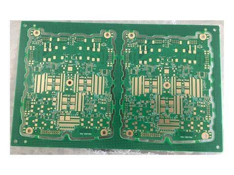
Manufacturing Process Of MFS Flexible PCB
The manufacturing process of MFS flexible printed circuit boards (PCBs) is a sophisticated and intricate procedure that requires precision and expertise. MFS, or Multi-Flex Systems, flexible PCBs are designed to meet the demands of modern electronic devices, which require compact, lightweight, and highly reliable components. The process begins with the selection of appropriate materials, which is crucial for ensuring the flexibility and durability of the final product. Polyimide films are commonly used as the substrate material due to their excellent thermal stability and mechanical properties. These films serve as the foundation upon which the circuit is built.
Once the substrate material is selected, the next step involves the application of a conductive layer, typically copper, onto the substrate.
This is achieved through a process known as electroless plating, which deposits a thin layer of copper onto the polyimide film. Following this, an additional layer of copper is added through electroplating to achieve the desired thickness. This dual-layer approach ensures that the conductive paths are robust enough to handle the electrical demands of the circuit while maintaining flexibility.
Subsequently, the circuit pattern is defined using a photolithographic process.
A photoresist material is applied over the copper layer, and the desired circuit pattern is transferred onto the photoresist using ultraviolet light. The areas exposed to the light become hardened, while the unexposed areas remain soft and are subsequently removed, revealing the underlying copper. This step is critical as it determines the precise layout of the circuit paths.
Following the patterning, the exposed copper is etched away using a chemical solution, leaving behind only the copper traces that form the circuit.
This etching process must be carefully controlled to ensure that the copper traces are not undercut or damaged, which could compromise the circuit’s performance. After etching, the remaining photoresist is stripped away, revealing the completed circuit pattern on the flexible substrate.
To protect the circuit and enhance its performance, a solder mask is applied over the copper traces.
This protective layer prevents oxidation and short circuits, while also providing a surface for soldering components onto the PCB. The solder mask is typically applied using a screen-printing process, which ensures precise coverage and alignment with the underlying circuit.
The final stages of the manufacturing process involve the addition of surface finishes and the assembly of components.
Surface finishes, such as immersion gold or silver, are applied to the exposed copper pads to improve solderability and protect against corrosion. Component assembly is then carried out using surface-mount technology (SMT), where components are placed onto the PCB and soldered in place using reflow soldering techniques.
Throughout the manufacturing process, rigorous quality control measures are implemented to ensure that each MFS flexible PCB meets the required specifications and performance standards. This includes electrical testing to verify circuit continuity and functionality, as well as visual inspections to detect any defects or irregularities.
In conclusion, the manufacturing process of MFS flexible PCBs is a complex and meticulous procedure that combines advanced materials and technologies to produce high-quality, reliable circuit boards. By understanding each step of the process, manufacturers can ensure that their products meet the ever-evolving demands of the electronics industry, providing the flexibility and performance required for modern applications.
Future Trends In MFS Flexible PCB Technology
The realm of flexible printed circuit boards (PCBs) is undergoing a transformative evolution, with MFS (Multi-Functional Substrate) flexible PCBs at the forefront of this technological advancement. As industries increasingly demand more compact, efficient, and versatile electronic solutions, the future trends in MFS flexible PCB technology are poised to redefine the landscape of electronic design and manufacturing. This article explores the emerging trends and potential future developments in this dynamic field.
To begin with, the miniaturization of electronic components continues to be a driving force behind the evolution of MFS flexible PCBs.
As devices become smaller and more complex, the need for PCBs that can accommodate intricate circuitry within limited spaces becomes paramount. MFS flexible PCBs offer a solution by providing a substrate that can bend and fold, allowing for more compact and lightweight designs. This trend is particularly evident in the consumer electronics sector, where the demand for wearable technology and portable devices is surging. Consequently, manufacturers are investing in research and development to enhance the flexibility and durability of these substrates, ensuring they can withstand the rigors of everyday use.
Moreover, the integration of advanced materials into MFS flexible PCBs is another trend shaping the future of this technology.
The use of novel materials such as conductive polymers, graphene, and other nanomaterials is being explored to improve the electrical performance and thermal management of flexible PCBs. These materials not only enhance the conductivity and heat dissipation capabilities of the circuits but also contribute to the overall flexibility and resilience of the substrate. As a result, MFS flexible PCBs are becoming increasingly suitable for high-performance applications, including those in the automotive and aerospace industries, where reliability and efficiency are critical.
In addition to material advancements, the incorporation of smart technologies into MFS flexible PCBs is gaining momentum.
The integration of sensors, actuators, and communication modules directly onto the PCB substrate is enabling the development of smart systems that can interact with their environment and provide real-time data. This trend is particularly relevant in the context of the Internet of Things (IoT), where interconnected devices require seamless communication and data exchange. By embedding these functionalities into the PCB itself, manufacturers can create more streamlined and efficient systems, reducing the need for additional components and simplifying the overall design.
Furthermore, the push towards sustainable and environmentally friendly manufacturing processes is influencing the future of MFS flexible PCB technology.
As environmental concerns become more pressing, there is a growing emphasis on developing PCBs that are not only high-performing but also eco-friendly. This includes the use of recyclable materials, reducing waste during production, and implementing energy-efficient manufacturing techniques. By prioritizing sustainability, the industry is not only addressing environmental challenges but also meeting the increasing consumer demand for greener products.
In conclusion, the future trends in MFS flexible PCB technology are characterized by a convergence of miniaturization, material innovation, smart integration, and sustainability. As these trends continue to evolve, they promise to unlock new possibilities in electronic design and manufacturing, paving the way for more advanced, efficient, and environmentally conscious solutions. The ongoing advancements in this field underscore the importance of continued research and collaboration among industry stakeholders
to fully realize the potential of MFS flexible PCBs in shaping the future of electronics.