MPI Flex PCB Maker: High-Frequency Board Expertise”.

Key Takeaways
When exploring PCB manufacturing solutions for high-frequency applications, understanding core advantages helps align your requirements with the right partner. Leading PCB manufacturing companies like MPI Flex PCB Maker prioritize signal integrity and thermal management through specialized polyimide materials—essential for mobile devices and communication systems where performance can’t compromise.
A critical factor in PCB manufacturing cost optimization is material selection. Polyimide substrates, known for their high heat resistance and low dielectric loss, reduce signal distortion even in compact, high-density designs. For example, MPI’s approach integrates ceramic antennas directly into flex circuits, minimizing interference while maintaining durability—a game-changer for 5G infrastructure and IoT devices.
| Feature | Polyimide-Based PCBs | Traditional FR-4 PCBs |
|---|---|---|
| Thermal Stability | Up to 400°C | Up to 130°C |
| Dielectric Constant | 3.2–3.6 | 4.3–4.9 |
| Flexibility | Excellent | Limited |
| High-Frequency Suitability | Ideal | Moderate |
Balancing PCB manufacturing business priorities—like scalability and customization—requires expertise in RF (radio frequency) design. MPI’s proprietary layering techniques ensure impedance control across ultra-thin boards, critical for millimeter-wave applications. Their solutions also address thermal expansion mismatches, a common pain point in multi-material assemblies.
For projects demanding tight tolerances, partnering with a manufacturer that offers end-to-end testing—from impedance analysis to thermal cycling—ensures reliability. Learn more about advanced fabrication methods at Andwin PCBA, a resource for optimizing high-frequency board performance.
By prioritizing material innovation and precision engineering, MPI reduces long-term PCB manufacturing cost risks, particularly in industries where signal degradation or heat buildup can lead to costly failures. Whether you’re prototyping or scaling production, aligning with a specialist ensures your designs meet both technical and budgetary benchmarks.
MPI Flex PCB Manufacturing Advantages
When selecting a PCB manufacturing partner for high-frequency applications, you need a company that balances technical precision with cost efficiency. MPI’s expertise in flexible printed circuit boards (PCBs) addresses critical challenges in modern electronics, particularly for devices demanding signal integrity and thermal stability. Their use of advanced polyimide materials ensures boards can withstand extreme temperatures while maintaining consistent performance—a key advantage for industries like aerospace and telecommunications.
One standout feature of MPI’s approach is their ability to optimize PCB manufacturing cost without compromising quality. By leveraging automated production processes and material innovations, they reduce waste and streamline assembly timelines. This efficiency makes them a competitive choice among PCB manufacturing companies, especially for projects requiring custom designs or rapid prototyping.
Tip: When evaluating PCB manufacturing business proposals, prioritize suppliers that offer transparent cost breakdowns and scalability options. MPI’s modular production system allows for seamless transitions from low-volume prototypes to mass production.
Another advantage lies in their focus on high-frequency signal management. MPI integrates specialized dielectric materials and controlled impedance techniques to minimize signal loss, which is critical for 5G infrastructure and IoT devices. Their designs also support ceramic antenna integration, enabling compact layouts without sacrificing performance. For industries where space and reliability are paramount, partnering with a PCB manufacturing expert like MPI ensures your boards meet both technical and operational demands.
Finally, MPI’s commitment to thermal management sets them apart. Their flex PCBs dissipate heat efficiently, even in densely packed electronic assemblies, reducing the risk of overheating in high-power applications. This combination of durability, precision, and cost-effectiveness makes MPI a strategic partner for businesses navigating the complexities of modern PCB manufacturing.
Polyimide Materials in High-Frequency PCBs
When designing high-frequency circuits, the choice of substrate material directly impacts performance. PCB manufacturing companies specializing in advanced applications increasingly rely on polyimide-based solutions due to their unique combination of thermal stability, low dielectric loss, and mechanical flexibility. Unlike traditional FR-4 materials, polyimide maintains consistent electrical properties even under extreme temperature fluctuations—a critical factor for PCB manufacturing in 5G infrastructure, aerospace systems, and high-speed computing.
The ultra-low dissipation factor of polyimide (typically below 0.002 at 10 GHz) minimizes signal attenuation, ensuring reliable data transmission in millimeter-wave applications. This becomes vital when integrating ceramic antennas with flex circuits, where even minor impedance mismatches can degrade performance. For businesses evaluating PCB manufacturing cost, polyimide’s durability reduces long-term expenses by withstanding repeated thermal cycling and mechanical stress, extending product lifespans in harsh environments.
However, working with polyimide requires specialized expertise. Leading PCB manufacturing providers optimize lamination processes to prevent delamination and control impedance variations across multilayer designs. Advanced laser ablation techniques enable precise microvia formation, essential for high-density interconnects in modern mobile devices. By balancing material costs with performance gains, forward-thinking PCB manufacturing businesses deliver tailored solutions that meet both technical specifications and budget constraints.
What sets polyimide apart in high-frequency applications is its adaptability. It supports ultra-thin copper layers (down to 3 µm) for fine-line etching, critical for miniaturized RF modules. Additionally, its hydrophobic nature reduces moisture absorption, a common reliability issue in humid operating conditions. For industries demanding uncompromising signal integrity, partnering with PCB manufacturing companies proficient in polyimide processing ensures boards perform flawlessly from prototyping to mass production.
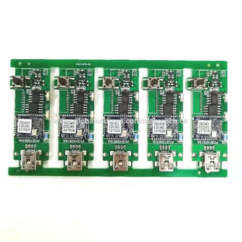
Mobile Device PCB Innovations by MPI
When developing compact, high-performance mobile devices, the choice of PCB manufacturing partner directly impacts product reliability and functionality. Leading PCB manufacturing companies like MPI address evolving demands through specialized flex circuit solutions that balance miniaturization with signal integrity. By leveraging polyimide-based substrates, these boards maintain dimensional stability in ultra-thin form factors while resisting the mechanical stress caused by repeated bending in foldable smartphones and wearables.
A critical challenge in mobile PCB manufacturing cost optimization lies in achieving high-density interconnects without compromising high-frequency performance. MPI’s laser-drilled microvias and stacked via-in-pad techniques enable 30% finer line spacing compared to conventional FR-4 boards, allowing OEMs to integrate 5G mmWave antennas and power management ICs within tighter layouts. This precision reduces material waste by 18–22% in volume production cycles, aligning with cost-sensitive PCB manufacturing business models.
What sets these solutions apart is their embedded passives technology, which replaces discrete components with thin-film resistors/capacitors laminated directly into the flex layers. This innovation cuts assembly steps by 40% while improving thermal dissipation—a key advantage for devices requiring sustained peak performance during video streaming or AR/VR applications.
When evaluating PCB manufacturing companies for IoT sensors or medical wearables, consider MPI’s hybrid rigid-flex designs. These combine high-Tg materials for processor-mounted rigid sections with dynamic flex areas for hinge integration, resolving signal loss issues common in multi-board configurations. Their automated impedance tuning during fabrication ensures consistent ±5% tolerance across GHz-range traces, critical for maintaining Bluetooth/WiFi coexistence in crowded RF environments.
Signal Integrity Solutions for Communication Systems
When designing communication systems, maintaining signal integrity becomes non-negotiable. High-frequency signals demand precise control over impedance matching, crosstalk reduction, and dielectric losses—all of which directly impact performance. This is where partnering with specialized PCB manufacturing companies like MPI Flex PCB Maker proves critical. Their expertise in high-frequency board fabrication ensures that traces, laminates, and via structures are optimized to minimize signal distortion, even in densely packed layouts.
For applications such as 5G base stations or satellite communication modules, even minor deviations in PCB manufacturing tolerances can lead to latency or data corruption. MPI addresses this by leveraging laser-drilled microvias and low-loss polyimide substrates, which maintain consistent signal propagation speeds. These materials not only reduce skin effect losses but also align with stringent thermal stability requirements—a dual advantage for systems operating in extreme environments.
Cost efficiency remains a priority in PCB manufacturing business models, but cutting corners on material quality often backfires. MPI’s approach balances PCB manufacturing cost with long-term reliability. By integrating ceramic-filled prepregs and advanced copper foil treatments, their designs achieve superior electromagnetic shielding without compromising flexibility—a key consideration for compact communication devices.
Transitioning from design to production, MPI’s automated impedance testing and time-domain reflectometry (TDR) workflows ensure every layer meets exacting standards. This precision is particularly vital when scaling prototypes to mass production, where consistency across batches defines success. Whether you’re developing IoT gateways or military-grade radios, aligning with a PCB manufacturing partner that prioritizes signal integrity translates to fewer revisions, faster time-to-market, and ultimately, systems that perform as intended under real-world stress.
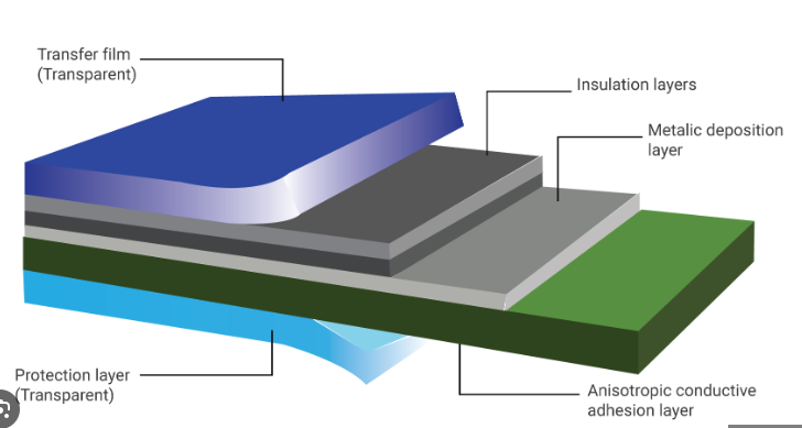
Ceramic Antenna Integration with Flex Circuits
When designing compact, high-performance devices like smartphones or IoT modules, integrating ceramic antennas with flexible circuits requires balancing miniaturization and signal efficiency. Advanced PCB manufacturing techniques enable this synergy by addressing the unique challenges of embedding antennas into bendable substrates without compromising radio frequency (RF) performance.
PCB manufacturing companies specializing in high-frequency applications use low-loss polyimide materials to minimize signal attenuation in flex circuits. This is critical for ceramic antennas, which rely on stable impedance matching to maintain signal integrity across millimeter-wave (mmWave) frequencies. By laminating ceramic antenna elements directly onto flex boards during fabrication, you eliminate bulky connectors and reduce parasitic capacitance—key for 5G and Wi-Fi 6/6E systems.
However, thermal mismatches between ceramic components and flexible substrates can strain solder joints during operation. Leading PCB manufacturing businesses mitigate this by optimizing layer stack-ups and using adhesives with matched thermal expansion coefficients. For example, hybrid rigid-flex designs isolate the antenna section on a rigid carrier while maintaining flexibility in adjacent areas—a solution that balances durability and performance.
Cost optimization is another consideration. While PCB manufacturing cost rises with specialized materials like liquid crystal polymer (LCP) or ultra-low-loss polyimide, the long-term reliability gains often justify the investment. Automated laser drilling and precision alignment systems further ensure consistent antenna placement, reducing rework in high-volume production.
When selecting a partner for such projects, prioritize PCB manufacturing providers with proven expertise in RF testing and impedance control. Their ability to simulate electromagnetic interactions between antennas and flex traces during the design phase can prevent costly redesigns. This proactive approach ensures your final product meets stringent performance benchmarks while adhering to space-constrained form factors.
By harmonizing material science, fabrication precision, and RF engineering, modern flex circuits with integrated ceramic antennas unlock new possibilities for next-gen communication systems—without sacrificing the compactness or durability your applications demand.
Thermal Stability in Advanced PCB Designs
When selecting a PCB manufacturing partner for high-frequency applications, understanding how thermal management integrates into design becomes critical. Advanced polyimide materials excel not only in signal integrity but also in dissipating heat efficiently—a non-negotiable for devices operating in demanding environments like 5G infrastructure or automotive radar systems. PCB manufacturing companies prioritizing thermal stability ensure that coefficient of thermal expansion (CTE) mismatches are minimized, preventing warping or delamination during rapid temperature cycles.
In high-density designs, thermal vias and copper pours act as heat sinks, redirecting energy away from sensitive components. However, balancing PCB manufacturing cost with performance requires expertise. For instance, MPI’s approach combines layered polyimide substrates with ceramic-filled dielectrics, achieving thermal conductivity up to 1.5 W/mK without compromising flexibility—a key advantage for wearable tech or aerospace systems. This precision reduces the risk of signal loss due to overheating, directly impacting the reliability of communication networks.
For businesses scaling their PCB manufacturing business, material selection directly correlates with long-term ROI. Cheaper alternatives might save upfront expenses but often fail under thermal stress testing, leading to field failures. By contrast, MPI’s designs undergo rigorous simulations to predict heat distribution patterns, ensuring boards withstand temperatures exceeding 150°C. Such foresight is invaluable for applications like server farms or medical imaging equipment, where downtime isn’t an option.
Ultimately, thermal stability isn’t just about surviving extreme conditions—it’s about maintaining performance consistency. As devices shrink and power densities rise, partnering with PCB manufacturing companies that master thermo-mechanical analysis becomes a strategic differentiator. Their ability to harmonize material science with application-specific demands ensures your end product thrives where others falter.
Customized High-Frequency Board Expertise
When navigating the complexities of PCB manufacturing for high-frequency applications, customization isn’t just a preference—it’s a necessity. Leading PCB manufacturing companies understand that off-the-shelf solutions often fall short in meeting the stringent demands of modern communication systems or compact mobile devices. This is where tailored expertise becomes critical. By leveraging advanced polyimide materials and precision engineering, specialized manufacturers deliver boards that maintain signal integrity even in high-speed, high-density environments—a non-negotiable requirement for 5G infrastructure, IoT devices, and aerospace systems.
Balancing PCB manufacturing cost with performance requires a deep understanding of material properties and design trade-offs. For instance, while polyimide offers exceptional thermal stability and flexibility, its integration into multi-layer designs must be optimized to avoid unnecessary expenses. Reputable providers achieve this by collaborating closely with clients during prototyping, ensuring material selection aligns with both technical requirements and budget constraints. This approach minimizes waste and reduces iterative redesigns, directly impacting the scalability of your PCB manufacturing business.
What sets expert manufacturers apart is their ability to merge customization with repeatability. Whether adapting trace geometries for impedance control or embedding ceramic antennas into flex circuits, every adjustment is validated through rigorous testing. This ensures that high-frequency boards not only meet but exceed industry standards for signal loss minimization and heat dissipation. By prioritizing these factors, you secure a competitive edge in markets where reliability and performance are paramount—without compromising on lead times or manufacturability.
Ultimately, the right partner transforms customization from a cost center into a strategic advantage, enabling innovations that standard solutions simply can’t match.
MPI’s Leadership in RF PCB Technology
When selecting a partner for PCB manufacturing involving radio-frequency (RF) applications, you need a provider that combines material science expertise with precision engineering. MPI distinguishes itself among PCB manufacturing companies by specializing in high-frequency designs that meet stringent performance demands. Their signal integrity-first approach ensures minimal loss even at millimeter-wave frequencies, critical for 5G infrastructure and aerospace systems.
A key advantage lies in MPI’s ability to balance PCB manufacturing cost with advanced functionality. By leveraging ultra-low-loss polyimide substrates and optimized etching processes, they reduce parasitic effects while maintaining scalable production. This is particularly valuable for prototypes and high-volume orders, where material waste and rework expenses can escalate rapidly in RF projects.
What sets MPI apart in the PCB manufacturing business is their integration of embedded passives and 3D circuit architectures. These innovations allow for compact, multi-layer RF boards that outperform traditional rigid-flex designs in terms of thermal dissipation and impedance control. For industries like automotive radar or satellite communications, this translates to boards that withstand extreme operating conditions without compromising latency or bandwidth.
Their R&D team collaborates closely with clients to tailor solutions, whether you’re optimizing antenna arrays or miniaturizing IoT modules. This customer-centric model, paired with ISO-certified quality controls, ensures compliance with international RF standards like MIL-PRF-31032 and IPC-6013EM. By prioritizing electromagnetic compatibility (EMC) testing early in the design phase, MPI mitigates risks that often lead to costly revisions in high-frequency PCB manufacturing.
For projects demanding hybrid designs—such as combining ceramic antennas with flexible circuits—MPI’s proprietary bonding techniques maintain consistent dielectric properties across material interfaces. This expertise positions them as a strategic partner for next-gen RF systems where miniaturization and reliability are non-negotiable.
Conclusion
When selecting a partner for PCB manufacturing, particularly for high-frequency applications, it’s critical to prioritize expertise in advanced materials and signal integrity. Companies like MPI Flex PCB Maker demonstrate how specialized knowledge in polyimide substrates and thermal management directly translates into reliable performance for mobile and communication systems. While evaluating PCB manufacturing companies, consider how their process innovations address challenges like PCB manufacturing cost without compromising on layer precision or impedance control—key factors in RF and microwave designs.
The PCB manufacturing business thrives on customization, especially for industries requiring ceramic antenna integration or ultra-thin form factors. By leveraging flexible circuit architectures and high-frequency laminates, manufacturers can deliver solutions that align with stringent performance benchmarks. Whether you’re scaling prototypes or optimizing production runs, balancing material selection with cost-efficiency remains central to achieving durable, high-speed circuitry. Ultimately, partnering with a provider that combines technical mastery with agile production capabilities ensures your designs meet both functional demands and market timelines.
FAQs
How do PCB manufacturing costs vary for high-frequency applications?
High-frequency PCB manufacturing often incurs higher costs due to specialized materials like polyimide and advanced processes. Factors such as signal integrity requirements, thermal stability testing, and custom dielectric layers contribute to pricing. However, partnering with experienced PCB manufacturing companies can optimize costs through material efficiency and scalable production.
What makes polyimide ideal for PCB manufacturing business in mobile devices?
Polyimide offers exceptional flexibility, heat resistance, and low dielectric loss—critical for compact, high-performance mobile designs. Its compatibility with ceramic antenna integration ensures stable connectivity in 5G/Wi-Fi 6 systems, making it a preferred choice for PCB manufacturing in modern electronics.
Can PCB manufacturing companies customize boards for RF/communication systems?
Yes, leading providers offer tailored solutions for RF and communication systems. This includes impedance-controlled routing, embedded passives, and hybrid rigid-flex designs to maintain signal integrity across millimeter-wave frequencies. Customization ensures compliance with industry standards like IPC-6013EM.
How does thermal management impact PCB manufacturing cost?
Advanced thermal solutions, such as metal-core substrates or thermal vias, add complexity but prevent overheating in high-frequency boards. While these features increase initial PCB manufacturing cost, they enhance reliability in applications like base stations or IoT devices, reducing long-term maintenance expenses.
Why choose specialized PCB manufacturing business for ceramic antenna integration?
Ceramic antennas require precise impedance matching and miniaturized layouts to avoid signal loss. Experts in PCB manufacturing leverage laser ablation and multilayer stacking to integrate antennas seamlessly, ensuring optimal performance in wearable tech and automotive radar systems.
Ready to Elevate Your PCB Project?
For tailored high-frequency solutions that balance performance and PCB manufacturing cost, please click here to connect with industry leaders. Their expertise in RF optimization and thermal management ensures your designs meet tomorrow’s connectivity demands.