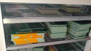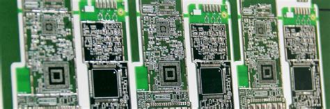
Multi layer in pcb
Advantages Of Multi-Layer PCBs In Modern Electronics
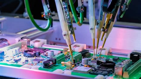
In the rapidly evolving landscape of modern electronics, the demand for more compact, efficient, and high-performing devices has led to significant advancements in printed circuit board (PCB) technology. Among these advancements, multi-layer PCBs have emerged as a pivotal innovation, offering numerous advantages that cater to the complex requirements of contemporary electronic devices. As we delve into the benefits of multi-layer PCBs, it becomes evident that their adoption is driven by the need for enhanced functionality and reliability in a wide array of applications.
To begin with, one of the most notable advantages of multi-layer PCBs is their ability to accommodate a higher density of components.
By stacking multiple layers of circuitry, these PCBs can support a greater number of connections and components within a smaller footprint. This is particularly beneficial in the design of compact devices such as smartphones, tablets, and wearable technology, where space is at a premium. The increased density not only allows for more complex circuitry but also contributes to the miniaturization of electronic devices, a trend that continues to dominate the industry.
Moreover, multi-layer PCBs offer improved electrical performance compared to their single-layer counterparts.
The additional layers provide more routing options, which can significantly reduce the length of electrical paths. This reduction in path length minimizes signal loss and electromagnetic interference, leading to better signal integrity and faster transmission speeds. Consequently, devices that rely on high-speed data processing, such as computers and telecommunications equipment, benefit greatly from the enhanced performance characteristics of multi-layer PCBs.
In addition to their superior electrical performance, multi-layer PCBs are known for their increased durability and reliability.
The multiple layers are bonded together with a strong adhesive and are often reinforced with materials such as fiberglass, which enhances the overall structural integrity of the board. This robust construction makes multi-layer PCBs less susceptible to damage from environmental factors such as heat, vibration, and mechanical stress. As a result, they are well-suited for use in demanding applications, including automotive, aerospace, and industrial electronics, where reliability is paramount.
Furthermore, the design flexibility offered by multi-layer PCBs is another significant advantage.
Designers have the freedom to incorporate a variety of components and functionalities into a single board, thanks to the additional layers. This flexibility allows for the integration of advanced features such as power management systems, RF modules, and complex signal processing units, all within a compact and efficient design. The ability to customize the board layout to meet specific application requirements is a key factor driving the widespread adoption of multi-layer PCBs in diverse industries.
Finally, it is important to consider the economic benefits associated with multi-layer PCBs.
While the initial manufacturing costs may be higher than those of single-layer boards, the long-term advantages often outweigh these costs. The increased functionality and reliability of multi-layer PCBs can lead to reduced maintenance and replacement expenses, as well as improved product performance and customer satisfaction. In a competitive market, these factors can provide a significant edge to manufacturers who choose to invest in multi-layer PCB technology.
In conclusion, the advantages of multi-layer PCBs in modern electronics are manifold, encompassing improved component density, superior electrical performance, enhanced durability, design flexibility, and economic benefits. As electronic devices continue to evolve and demand more sophisticated capabilities, multi-layer PCBs will undoubtedly play a crucial role in meeting these challenges, solidifying their position as an indispensable component in the future of electronics.

Design Considerations For Multi-Layer PCB Fabrication
In the realm of electronics, the design and fabrication of printed circuit boards (PCBs) are crucial for the development of efficient and compact electronic devices. Among the various types of PCBs, multi-layer PCBs have gained prominence due to their ability to accommodate complex circuitry within a limited space. As the demand for more sophisticated electronic devices continues to grow, understanding the design considerations for multi-layer PCB fabrication becomes increasingly important.
To begin with, one of the primary considerations in multi-layer PCB design is the selection of materials.
The choice of substrate material significantly impacts the board’s performance, thermal management, and overall reliability. Commonly used materials include FR-4, a glass-reinforced epoxy laminate, which offers a good balance between performance and cost. However, for applications requiring higher frequency or better thermal properties, materials such as polyimide or Rogers laminates may be preferred. The dielectric constant and loss tangent of these materials must be carefully evaluated to ensure signal integrity and minimize electromagnetic interference.
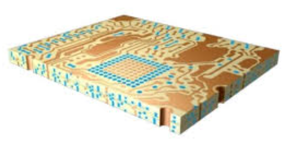
Transitioning to the layout design, the stack-up configuration of a multi-layer PCB is another critical factor.
The stack-up refers to the arrangement of conductive and insulating layers within the PCB. A well-designed stack-up can enhance signal integrity, reduce electromagnetic emissions, and improve power distribution. Typically, a multi-layer PCB consists of alternating layers of signal and power/ground planes. The placement of these layers should be strategically planned to minimize crosstalk and impedance mismatches. For instance, placing a ground plane adjacent to a signal layer can provide a return path for signals, thereby reducing electromagnetic interference.
Moreover, the routing of traces in a multi-layer PCB requires meticulous attention.
As the number of layers increases, so does the complexity of trace routing. Designers must ensure that traces are routed efficiently to avoid unnecessary vias, which can introduce parasitic inductance and capacitance. Additionally, differential pairs, which are commonly used for high-speed signals, should be routed with consistent spacing and length to maintain signal integrity. Employing design rules and constraints in PCB design software can aid in achieving optimal trace routing.
In addition to routing, the aspect of thermal management cannot be overlooked.
Multi-layer PCBs, with their dense circuitry, are prone to heat accumulation, which can adversely affect performance and reliability. Effective thermal management strategies, such as the use of thermal vias, heat sinks, and thermal pads, should be incorporated into the design. These measures help dissipate heat away from critical components, ensuring the longevity and stability of the device.
Furthermore, the consideration of manufacturing tolerances is essential in multi-layer PCB fabrication.
Variations in layer thickness, trace width, and spacing can occur during the manufacturing process, potentially leading to performance issues. Designers must account for these tolerances by specifying appropriate design margins and working closely with manufacturers to ensure that the fabricated PCB meets the intended specifications.
In conclusion, the design considerations for multi-layer PCB fabrication are multifaceted, encompassing material selection, stack-up configuration, trace routing, thermal management, and manufacturing tolerances. By carefully addressing these factors, designers can create multi-layer PCBs that meet the demands of modern electronic devices, providing enhanced performance, reliability, and functionality. As technology continues to evolve, staying abreast of advancements in materials and design techniques will be crucial for the successful development of next-generation electronic products.
Cost-Effectiveness Of Multi-Layer PCBs In High-Density Applications
In the realm of modern electronics, the demand for compact, efficient, and high-performance devices has led to significant advancements in printed circuit board (PCB) technology. Among these advancements, multi-layer PCBs have emerged as a pivotal solution, particularly in high-density applications. These PCBs, characterized by multiple layers of conductive material separated by insulating substrates, offer a myriad of benefits that contribute to their cost-effectiveness in complex electronic systems.
To begin with, multi-layer PCBs enable the integration of a greater number of components within a limited space.
This is particularly advantageous in high-density applications where space constraints are a critical consideration. By stacking multiple layers, designers can achieve a higher component density without increasing the overall footprint of the PCB. Consequently, this leads to a reduction in the size and weight of the final product, which is a crucial factor in industries such as consumer electronics, aerospace, and telecommunications.
Moreover, the use of multi-layer PCBs enhances the electrical performance of the circuit.
The additional layers allow for more intricate routing of electrical connections, which minimizes the length of signal paths and reduces the potential for interference. This is especially important in high-frequency applications where signal integrity is paramount. The improved electrical performance not only enhances the functionality of the device but also contributes to its reliability and longevity, thereby reducing the need for frequent repairs or replacements.
In addition to performance benefits, multi-layer PCBs offer significant cost advantages over their single-layer counterparts in high-density applications.
While the initial manufacturing cost of multi-layer PCBs may be higher due to the complexity of their design and fabrication, the long-term savings are substantial. The ability to consolidate multiple functions onto a single board reduces the need for additional components and interconnections, which in turn lowers the overall material and assembly costs. Furthermore, the enhanced reliability and performance of multi-layer PCBs can lead to a reduction in warranty claims and maintenance expenses, providing further cost savings over the product’s lifecycle.
Another aspect of cost-effectiveness is the potential for economies of scale in the production of multi-layer PCBs.
As demand for high-density applications continues to grow, manufacturers are increasingly investing in advanced fabrication technologies that streamline the production process. This not only reduces the per-unit cost of multi-layer PCBs but also shortens lead times, allowing for faster time-to-market for new products. Consequently, companies can achieve a competitive edge by leveraging the cost efficiencies associated with large-scale production.
Furthermore, the versatility of multi-layer PCBs makes them an attractive option for a wide range of applications, from simple consumer gadgets to complex industrial systems. This adaptability ensures that investments in multi-layer PCB technology can be amortized across multiple projects, further enhancing their cost-effectiveness. As technology continues to evolve, the ability to quickly adapt to new requirements and integrate emerging technologies becomes increasingly valuable.
In conclusion, the cost-effectiveness of multi-layer PCBs in high-density applications is underscored by their ability to optimize space, enhance electrical performance, and reduce overall costs through component consolidation and economies of scale. As industries continue to push the boundaries of what is possible with electronic devices, multi-layer PCBs will undoubtedly play a crucial role in meeting the demands of tomorrow’s high-density applications.
Thermal Management Strategies In Multi-Layer PCB Design
In the realm of electronics, the design of printed circuit boards (PCBs) plays a crucial role in determining the performance and reliability of electronic devices. As technology advances, the demand for more compact and efficient devices has led to the development of multi-layer PCBs. These complex structures, consisting of multiple layers of conductive material separated by insulating layers, offer numerous advantages, including increased circuit density and improved electrical performance. However, with these benefits come challenges, particularly in the area of thermal management. Effective thermal management strategies are essential to ensure the longevity and functionality of multi-layer PCBs.
One of the primary challenges in multi-layer PCB design is the dissipation of heat generated by electronic components.
As devices become more powerful, they tend to generate more heat, which can lead to overheating and potential failure if not properly managed. To address this issue, designers must employ a variety of thermal management strategies. One such strategy involves the use of thermal vias, which are small, plated holes that connect different layers of the PCB. These vias facilitate the transfer of heat from the surface of the board to the inner layers, where it can be more effectively dissipated. By strategically placing thermal vias near heat-generating components, designers can significantly enhance the thermal performance of the PCB.
In addition to thermal vias, the selection of materials plays a pivotal role in thermal management.
the choice of substrate material can greatly influence the thermal conductivity of the PCB. Materials with high thermal conductivity, such as aluminum or copper, are often used to improve heat dissipation. Furthermore, the use of thermal interface materials (TIMs) can enhance the thermal connection between components and the PCB, further aiding in heat transfer. These materials, which include thermal pads and pastes, fill the microscopic air gaps between surfaces, reducing thermal resistance and improving overall heat conduction.
Another effective strategy involves the optimization of the PCB layout.
By carefully arranging components and traces, designers can minimize heat accumulation in specific areas. For instance, placing high-power components away from each other and ensuring adequate spacing can prevent localized hotspots. Additionally, the use of copper planes, which are large areas of copper on a PCB layer, can help distribute heat more evenly across the board. These planes act as heat spreaders, reducing the thermal gradient and preventing excessive temperature rise in any one area.
Moreover, the integration of active cooling solutions, such as heat sinks and fans, can further enhance thermal management in multi-layer PCBs.
Heat sinks, which are typically made of metal, are attached to heat-generating components to increase the surface area available for heat dissipation. Fans, on the other hand, provide forced air circulation, which can significantly improve the cooling efficiency of the system. While these solutions add complexity and cost to the design, they are often necessary for high-performance applications where passive cooling methods alone are insufficient.
In conclusion, the design of multi-layer PCBs requires careful consideration of thermal management strategies to ensure optimal performance and reliability. By employing a combination of thermal vias, material selection, layout optimization, and active cooling solutions, designers can effectively manage heat dissipation in these complex structures. As electronic devices continue to evolve, the importance of innovative thermal management techniques in multi-layer PCB design will only grow, underscoring the need for ongoing research and development in this critical area.