Multilayer organic pcb
Advantages Of Multilayer Organic PCBs In Modern Electronics
Multilayer organic printed circuit boards (PCBs) have become a cornerstone in the advancement of modern electronics, offering a multitude of advantages that cater to the ever-evolving demands of technology. As electronic devices continue to shrink in size while increasing in functionality, the need for more sophisticated and efficient circuit board designs has become paramount. Multilayer organic PCBs, with their unique composition and structure, provide a solution that addresses these challenges effectively.
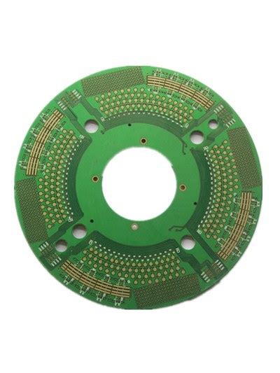
One of the primary advantages of multilayer organic PCBs is their ability to support high-density interconnections.
By stacking multiple layers of circuitry, these PCBs can accommodate a greater number of connections within a smaller footprint. This is particularly beneficial in applications where space is at a premium, such as in smartphones, tablets, and other portable devices. The compact nature of multilayer PCBs not only allows for more complex circuitry but also contributes to the miniaturization of electronic devices, a trend that continues to dominate the consumer electronics market.
In addition to their space-saving benefits, multilayer organic PCBs offer enhanced electrical performance.
The use of multiple layers allows for the separation of power and ground planes, which helps to reduce electromagnetic interference (EMI) and improve signal integrity. This is crucial in high-speed applications where signal clarity and reliability are essential. Furthermore, the ability to incorporate advanced materials and design techniques in multilayer PCBs enables the support of higher frequencies and faster data transmission rates, making them ideal for cutting-edge technologies such as 5G networks and advanced computing systems.
Another significant advantage of multilayer organic PCBs is their mechanical stability and durability.
The layered construction provides inherent strength, which enhances the board’s resistance to bending and warping. This robustness is particularly important in applications that involve harsh environmental conditions or mechanical stress, such as automotive and aerospace industries. Moreover, the use of organic materials in these PCBs contributes to their lightweight nature, which is a critical factor in applications where weight reduction is a priority.
The versatility of multilayer organic PCBs also extends to their design flexibility.
Engineers can tailor the number of layers and the arrangement of components to meet specific design requirements, allowing for customized solutions that optimize performance and functionality. This adaptability is invaluable in the development of innovative products that require unique configurations and specialized features.
Furthermore, the manufacturing process of multilayer organic PCBs has evolved to become more cost-effective and environmentally friendly.
Advances in fabrication techniques have reduced production costs, making these sophisticated boards more accessible to a wider range of applications. Additionally, the use of organic materials aligns with the growing emphasis on sustainability in the electronics industry, as they are generally more eco-friendly compared to their inorganic counterparts.
In conclusion, the advantages of multilayer organic PCBs in modern electronics are manifold, encompassing high-density interconnections, enhanced electrical performance, mechanical stability, design flexibility, and cost-effectiveness. As technology continues to advance, the role of these PCBs in enabling the development of smaller, faster, and more efficient electronic devices will undoubtedly become even more significant. Their ability to meet the complex demands of contemporary applications ensures that multilayer organic PCBs will remain a vital component in the future of electronics.
Design Considerations For Multilayer Organic PCBs
When designing multilayer organic printed circuit boards (PCBs), several critical considerations must be taken into account to ensure optimal performance and reliability. As the demand for more compact and efficient electronic devices grows, multilayer PCBs have become increasingly popular due to their ability to support complex circuitry within a reduced footprint. However, the design of these PCBs requires meticulous attention to detail, particularly when using organic materials, which offer unique advantages and challenges.
To begin with, the selection of materials is a fundamental aspect of multilayer organic PCB design.
Organic substrates, such as polyimide and liquid crystal polymer, are favored for their flexibility, lightweight nature, and excellent electrical properties. These materials are particularly advantageous in applications where weight and space are critical constraints, such as in aerospace and portable consumer electronics. However, designers must carefully consider the thermal and mechanical properties of these materials, as they can significantly influence the board’s performance under various environmental conditions.
Transitioning from material selection to layer configuration, the number of layers in a multilayer PCB is a crucial factor that impacts both the complexity and functionality of the board.
Designers must strike a balance between the desired electrical performance and the physical limitations of the board. More layers can accommodate more complex circuits and improve signal integrity by providing dedicated ground and power planes. However, increasing the number of layers also raises manufacturing costs and can complicate the fabrication process. Therefore, a thorough analysis of the circuit requirements and cost constraints is essential during the design phase.
Furthermore, signal integrity is a paramount consideration in multilayer organic PCB design.
As electronic devices operate at higher frequencies, issues such as crosstalk, electromagnetic interference, and signal attenuation become more pronounced. To mitigate these issues, designers must employ strategies such as controlled impedance routing, differential pair routing, and the use of ground planes to shield sensitive signals. Additionally, careful attention must be paid to the placement of vias, as they can introduce unwanted parasitic inductance and capacitance, potentially degrading signal quality.
In addition to signal integrity, thermal management is another critical aspect that cannot be overlooked.
Organic materials typically have lower thermal conductivity compared to their inorganic counterparts, making effective heat dissipation a challenge. Designers must incorporate thermal vias, heat sinks, and other cooling mechanisms to ensure that the board operates within safe temperature limits. This is particularly important in high-power applications where excessive heat can lead to component failure and reduced reliability.
Moreover, manufacturability is an essential consideration in the design of multilayer organic PCBs.
The choice of materials, layer count, and design complexity can all influence the ease of fabrication and assembly. Designers must work closely with manufacturers to ensure that the design is compatible with available fabrication technologies and processes. This collaboration can help identify potential issues early in the design process, reducing the risk of costly redesigns and production delays.
In conclusion, the design of multilayer organic PCBs involves a delicate balance of material selection, layer configuration, signal integrity, thermal management, and manufacturability. By carefully considering these factors, designers can create PCBs that meet the demanding requirements of modern electronic devices while maintaining reliability and cost-effectiveness. As technology continues to advance, the importance of thoughtful and informed PCB design will only grow, underscoring the need for expertise and innovation in this critical field.
Manufacturing Process Of Multilayer Organic PCBs
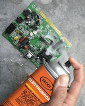
The manufacturing process of multilayer organic printed circuit boards (PCBs) is a sophisticated and intricate procedure that requires precision and expertise. These PCBs are integral to modern electronics, providing the necessary framework for complex circuitry in a compact form. The process begins with the selection of suitable materials, primarily organic substrates, which are chosen for their excellent electrical insulation properties and flexibility. These materials are typically composed of epoxy resins reinforced with glass fibers, offering a balance of durability and performance.
Once the materials are selected, the next step involves the creation of individual layers.
Each layer is meticulously designed to accommodate specific circuit patterns, which are transferred onto the substrate using advanced photolithography techniques. This process involves coating the substrate with a photosensitive material, exposing it to ultraviolet light through a mask that defines the circuit pattern, and then developing the image to reveal the desired circuitry. The precision of this step is crucial, as it determines the accuracy and functionality of the final PCB.
Following the patterning of individual layers, the process advances to the stacking and bonding phase.
Here, the patterned layers are aligned and laminated together under high pressure and temperature. This step is critical, as it ensures the mechanical integrity and electrical connectivity of the multilayer structure. The alignment must be exact to prevent any misregistration, which could lead to circuit failures. The bonding process also involves the use of adhesive materials that facilitate the fusion of layers while maintaining electrical isolation between them.
After the layers are bonded, the next stage involves drilling holes, known as vias, which serve as interconnections between different layers.
These vias are created using precision drilling techniques, often employing laser technology for microvias, which are essential for high-density interconnects. The drilled holes are then plated with a conductive material, typically copper, to establish electrical connections across the layers. This step is vital for the functionality of the multilayer PCB, as it enables the flow of electrical signals throughout the board.
Subsequently, the PCB undergoes a series of surface finishing processes to enhance its performance and reliability.
These processes include the application of solder masks, which protect the circuitry from environmental factors and prevent solder bridging during component assembly. Additionally, surface finishes such as immersion gold or silver are applied to improve solderability and protect the copper traces from oxidation.
Quality control is an integral part of the manufacturing process, ensuring that each PCB meets stringent industry standards.
This involves rigorous testing procedures, including electrical testing to verify circuit continuity and functionality, as well as visual inspections to detect any physical defects. Advanced testing methods, such as automated optical inspection and X-ray analysis, are employed to ensure the highest quality and reliability of the final product.
In conclusion, the manufacturing process of multilayer organic PCBs is a complex and precise operation that demands a high level of expertise and technological capability. From material selection to final testing, each step is meticulously executed to produce PCBs that meet the demanding requirements of modern electronic applications. As technology continues to evolve, the processes and materials used in PCB manufacturing are likely to advance, further enhancing the capabilities and applications of these essential components in the electronics industry.
Applications Of Multilayer Organic PCBs In Emerging Technologies
Multilayer organic printed circuit boards (PCBs) have emerged as a pivotal component in the advancement of emerging technologies, offering a range of applications that are transforming various industries. As the demand for more compact, efficient, and versatile electronic devices continues to grow, multilayer organic PCBs provide a solution that meets these requirements through their unique structural and material properties. These PCBs are constructed using multiple layers of conductive and insulating materials, which are laminated together to form a single, cohesive unit. This design allows for increased circuit density and complexity, making them ideal for applications in cutting-edge technologies.
One of the primary applications of multilayer organic PCBs is in the field of telecommunications.
With the rapid expansion of 5G networks, there is a pressing need for components that can support higher frequencies and faster data transmission rates. Multilayer organic PCBs are well-suited for this purpose due to their ability to accommodate complex circuitry within a compact form factor. This capability is crucial for the development of smaller, more efficient base stations and mobile devices that are essential for the widespread deployment of 5G technology. Furthermore, the flexibility of organic materials allows for the creation of PCBs that can be integrated into a variety of form factors, including flexible and wearable devices, which are becoming increasingly popular in the telecommunications sector.
In addition to telecommunications, multilayer organic PCBs are making significant inroads in the automotive industry.
As vehicles become more reliant on electronic systems for everything from engine control to infotainment, the demand for reliable and efficient PCBs has grown exponentially. Multilayer organic PCBs offer the necessary durability and performance to withstand the harsh conditions often encountered in automotive environments. Moreover, they enable the integration of advanced features such as driver assistance systems, which require sophisticated electronic control units capable of processing large amounts of data in real-time. The ability to incorporate multiple layers of circuitry within a single board also facilitates the miniaturization of components, which is essential for the development of electric and autonomous vehicles.
The medical field is another area where multilayer organic PCBs are proving to be invaluable.
The trend towards miniaturization and portability in medical devices has created a demand for PCBs that can support complex functionalities within a small footprint. Multilayer organic PCBs meet this need by providing the necessary circuit density and flexibility to accommodate advanced medical technologies such as wearable health monitors and implantable devices. These PCBs are also used in imaging equipment and diagnostic tools, where their ability to support high-speed data processing and transmission is critical for accurate and timely results.
Moreover, the consumer electronics industry continues to benefit from the advancements in multilayer organic PCB technology.
As consumers demand more powerful and feature-rich devices, manufacturers are turning to these PCBs to deliver the performance and reliability required. From smartphones and tablets to smart home devices, multilayer organic PCBs enable the integration of multiple functionalities within a single device, enhancing user experience while maintaining a compact design.
In conclusion, the applications of multilayer organic PCBs in emerging technologies are vast and varied, spanning industries such as telecommunications, automotive, medical, and consumer electronics. Their ability to support complex circuitry within a compact and flexible form factor makes them an indispensable component in the development of next-generation technologies. As these industries continue to evolve, the role of multilayer organic PCBs is likely to expand further, driving innovation and enabling new possibilities in the realm of electronic devices.