Multilayer pcb basics
Introduction To Multilayer PCB Design
Multilayer printed circuit boards (PCBs) have become a cornerstone in the design and manufacturing of modern electronic devices, offering a compact and efficient solution for complex circuitry. As technology continues to advance, the demand for smaller, faster, and more reliable electronic devices has driven the evolution of PCB design from simple single-layer boards to intricate multilayer configurations. Understanding the basics of multilayer PCB design is essential for engineers and designers who aim to create sophisticated electronic systems.
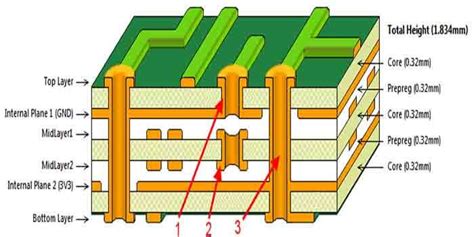
At its core, a multilayer PCB consists of multiple layers of conductive material, typically copper, separated by insulating layers known as dielectric materials.
These layers are laminated together under high pressure and temperature to form a single, cohesive unit. The primary advantage of this design is the ability to incorporate a greater number of circuits in a smaller footprint, which is crucial for modern electronics that require high functionality in compact forms.
One of the fundamental aspects of multilayer PCB design is the stack-up configuration, which refers to the arrangement and sequence of the conductive and insulating layers.
The stack-up is critical as it influences the electrical performance, signal integrity, and thermal management of the PCB. Designers must carefully consider the number of layers, the thickness of each layer, and the materials used to achieve the desired electrical characteristics and mechanical strength. Typically, a multilayer PCB can range from four to as many as fifty layers, depending on the complexity of the application.
Transitioning from single-layer to multilayer PCBs introduces several design challenges, particularly in terms of signal integrity and electromagnetic interference (EMI).
As signals traverse through multiple layers, they are susceptible to crosstalk and signal degradation. To mitigate these issues, designers employ techniques such as controlled impedance routing, differential pair routing, and the strategic placement of ground and power planes. These methods help maintain signal quality and reduce EMI, ensuring reliable performance in high-speed applications.
Moreover, the choice of materials plays a pivotal role in multilayer PCB design.
The dielectric material must possess suitable electrical properties, such as dielectric constant and loss tangent, to support high-frequency signals. Additionally, thermal management is a critical consideration, as multilayer PCBs can generate significant heat due to their dense circuitry. Materials with high thermal conductivity and the incorporation of thermal vias are often used to dissipate heat effectively, preventing damage to the components and ensuring longevity.
Another important aspect of multilayer PCB design is the manufacturing process, which is inherently more complex than that of single-layer boards.
The precision required in aligning and laminating multiple layers necessitates advanced fabrication techniques and equipment. Furthermore, the inspection and testing of multilayer PCBs are more rigorous, as defects such as misalignment or delamination can compromise the entire board’s functionality.
In conclusion, multilayer PCB design is a sophisticated process that requires a deep understanding of electrical engineering principles, material science, and manufacturing techniques. As electronic devices continue to evolve, the demand for multilayer PCBs will only increase, driving further innovation in design and fabrication methods. By mastering the basics of multilayer PCB design, engineers and designers can create cutting-edge electronic systems that meet the ever-growing demands of modern technology.

Advantages Of Using Multilayer PCBs
Multilayer printed circuit boards (PCBs) have become a cornerstone in the design and manufacturing of modern electronic devices, offering a range of advantages that make them indispensable in various applications. As technology continues to advance, the demand for more compact, efficient, and powerful electronic devices has driven the evolution of PCBs from simple single-layer designs to complex multilayer configurations. Understanding the benefits of multilayer PCBs is crucial for engineers and designers who aim to optimize the performance and reliability of their electronic products.
One of the primary advantages of multilayer PCBs is their ability to support high-density designs.
By stacking multiple layers of circuitry, these PCBs can accommodate a greater number of components and connections within a smaller footprint. This is particularly beneficial in the development of compact devices such as smartphones, tablets, and wearable technology, where space is at a premium. The increased density not only allows for more complex functionality but also contributes to the miniaturization of electronic devices, a trend that continues to dominate the consumer electronics market.
In addition to supporting high-density designs, multilayer PCBs offer enhanced electrical performance.
The close proximity of the layers allows for shorter signal paths, which in turn reduces signal loss and improves overall signal integrity. This is especially important in high-speed applications where maintaining signal quality is critical. Furthermore, the ability to incorporate multiple ground and power planes within the PCB stack-up helps to minimize electromagnetic interference (EMI) and crosstalk between signals, ensuring reliable operation even in demanding environments.
Another significant advantage of multilayer PCBs is their inherent design flexibility.
The multiple layers provide designers with the freedom to implement complex routing schemes and integrate a variety of components and technologies. This flexibility is essential in the development of advanced electronic systems, such as those found in aerospace, automotive, and telecommunications industries, where intricate designs are often required to meet specific performance criteria. Moreover, the ability to incorporate different materials and technologies within the same PCB allows for the creation of hybrid solutions that can address unique design challenges.
The reliability and durability of multilayer PCBs are also noteworthy.
The use of multiple layers not only enhances the mechanical strength of the board but also provides redundancy in the event of a failure in one of the layers. This is particularly advantageous in mission-critical applications where system failure is not an option. Additionally, the advanced manufacturing processes used in the production of multilayer PCBs ensure high-quality construction, which translates to longer lifespans and reduced maintenance requirements.
While the benefits of multilayer PCBs are numerous, it is important to acknowledge that their complexity can lead to increased design and manufacturing costs. However, the advantages they offer in terms of performance, reliability, and design flexibility often outweigh these costs, making them a worthwhile investment for many applications. As electronic devices continue to evolve, the role of multilayer PCBs in enabling innovation and enhancing functionality will undoubtedly remain significant. By leveraging the unique benefits of multilayer PCBs, designers and engineers can continue to push the boundaries of what is possible in the world of electronics.

Common Materials Used In Multilayer PCBs
In the realm of electronics, multilayer printed circuit boards (PCBs) have become indispensable due to their ability to support complex circuitry in a compact form. Understanding the common materials used in multilayer PCBs is crucial for anyone involved in electronics design and manufacturing. These materials not only influence the performance and reliability of the PCBs but also affect their cost and manufacturability. As we delve into the materials commonly employed in multilayer PCBs, it is essential to consider both the conductive and insulating components that form the backbone of these intricate structures.
To begin with, the conductive layers in multilayer PCBs are typically made of copper.
Copper is favored for its excellent electrical conductivity, which ensures efficient signal transmission across the board. The copper layers are usually deposited onto a substrate through a process known as electroplating, which allows for precise control over the thickness of the conductive paths. The thickness of these copper layers can vary depending on the specific requirements of the PCB, with common thicknesses ranging from 0.5 to 2 ounces per square foot. This variability allows designers to tailor the electrical characteristics of the PCB to suit different applications.
Transitioning to the insulating materials, the most prevalent substrate used in multilayer PCBs is FR-4, a composite material made from woven fiberglass cloth with an epoxy resin binder.
FR-4 is highly regarded for its excellent mechanical strength, thermal resistance, and electrical insulation properties. These characteristics make it an ideal choice for a wide range of applications, from consumer electronics to industrial equipment. Moreover, FR-4 is relatively cost-effective, which contributes to its widespread use in the industry. However, for applications requiring higher performance, alternative materials such as polyimide or PTFE (polytetrafluoroethylene) may be employed. Polyimide offers superior thermal stability and flexibility, making it suitable for high-temperature environments, while PTFE is known for its low dielectric constant and loss tangent, which are advantageous in high-frequency applications.
In addition to the core materials, multilayer PCBs also incorporate various other materials to enhance their functionality.
For instance, solder masks are applied to protect the copper traces from oxidation and to prevent solder bridges during assembly. These masks are typically made from epoxy-based polymers and are available in different colors, with green being the most common. Furthermore, silkscreen layers are used to print component labels and other markings on the PCB surface, aiding in assembly and troubleshooting. The inks used for silkscreening are usually epoxy-based as well, ensuring durability and resistance to environmental factors.
As we consider the materials used in multilayer PCBs, it is important to recognize the role of adhesives in bonding the layers together.
Prepregs, which are sheets of fiberglass impregnated with resin, are commonly used for this purpose. During the lamination process, the prepregs are heated and pressed, causing the resin to flow and cure, thereby forming a strong bond between the layers. The choice of prepreg material can significantly impact the thermal and mechanical properties of the final PCB, making it a critical consideration in the design process.
In conclusion, the materials used in multilayer PCBs are integral to their performance and reliability. From the conductive copper layers to the insulating substrates and protective coatings, each material plays a vital role in ensuring the functionality of the PCB. By carefully selecting and combining these materials, designers can create PCBs that meet the specific demands of their applications, whether they require high-frequency performance, thermal stability, or cost-effectiveness. Understanding these materials is therefore essential for anyone involved in the design and manufacture of multilayer PCBs.
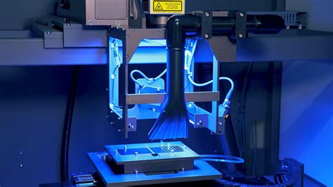
Manufacturing Process Of Multilayer PCBs
The manufacturing process of multilayer printed circuit boards (PCBs) is a complex and intricate procedure that requires precision and attention to detail. Multilayer PCBs, which consist of multiple layers of conductive material separated by insulating layers, are essential in modern electronics due to their ability to support more complex and compact designs. The process begins with the design phase, where engineers use specialized software to create a detailed blueprint of the PCB. This design includes the layout of the circuits, the placement of components, and the routing of electrical connections. Once the design is finalized, it is converted into a format suitable for manufacturing.
The next step involves the preparation of the raw materials.
Copper-clad laminates, which are sheets of insulating material coated with a thin layer of copper, are used as the base material. These laminates are cleaned and prepared to ensure that they are free from any contaminants that could affect the quality of the final product. Following this, the inner layers of the PCB are created. This involves printing the circuit pattern onto the copper surface using a photosensitive material. The board is then exposed to ultraviolet light, which hardens the exposed areas of the photosensitive material, leaving the circuit pattern intact. The unhardened material is then removed, revealing the copper circuit pattern.
Subsequently, the etched inner layers undergo a process called lamination.
During lamination, the inner layers are stacked together with layers of insulating material, known as prepreg, placed between them. This stack is then subjected to heat and pressure, causing the prepreg to melt and bond the layers together into a single, solid board. This step is crucial as it ensures the structural integrity of the multilayer PCB.
Once the lamination process is complete, the outer layers of the PCB are created.
This involves a similar process to that used for the inner layers, where the circuit pattern is printed, exposed, and etched onto the outer copper surfaces. After the outer layers are completed, the board undergoes drilling. Precision drilling machines create holes in the board for component leads and vias, which are used to connect the different layers of the PCB.
Following drilling, the board is plated with a thin layer of copper.
This plating process ensures that the drilled holes are conductive, allowing for electrical connections between the layers. The board is then coated with a layer of solder mask, which protects the copper circuits from oxidation and prevents solder bridges during component assembly. The solder mask is typically green, although other colors are also used.
Finally, the board undergoes a series of tests to ensure its functionality and reliability.
Electrical tests are conducted to verify that the circuits are correctly connected and that there are no short circuits or open circuits. Once the board passes these tests, it is ready for component assembly and integration into electronic devices.
In conclusion, the manufacturing process of multilayer PCBs is a meticulous and highly technical procedure that involves several critical steps. Each phase, from design to testing, plays a vital role in ensuring the quality and performance of the final product. As technology continues to advance, the demand for multilayer PCBs is expected to grow, further highlighting the importance of understanding this complex manufacturing process.