Multilayer pcb construction
Understanding The Basics Of Multilayer PCB Construction
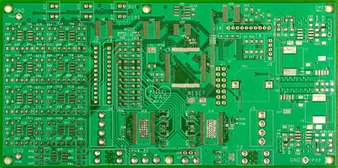
Multilayer printed circuit boards (PCBs) have become a cornerstone in the advancement of modern electronics, offering enhanced functionality and compactness that single-layer boards simply cannot achieve.
Understanding the basics of multilayer PCB construction is essential for anyone involved in electronics design and manufacturing. At its core, a multilayer PCB consists of multiple layers of conductive material, typically copper, separated by insulating layers known as substrates or dielectric materials. These layers are laminated together under high temperature and pressure to form a single, cohesive unit. The primary advantage of this construction is the ability to incorporate more complex circuits within a smaller footprint, which is crucial for the miniaturization of electronic devices.
The construction process begins with the design phase, where engineers use specialized software to create a detailed layout of the circuit.
This layout includes the placement of components, the routing of electrical connections, and the arrangement of the various layers. Once the design is finalized, it is transferred onto the individual layers of the PCB. Each layer is etched to remove excess copper, leaving behind the desired circuit pattern. This etching process is critical, as it ensures that the electrical pathways are precise and free from defects that could lead to short circuits or other malfunctions.
Following the etching process, the layers are aligned and laminated together.
This step is crucial, as any misalignment can result in connectivity issues or reduced performance. The lamination process involves applying heat and pressure to bond the layers, creating a solid and durable structure. The use of high-quality materials and precise manufacturing techniques is essential to ensure the reliability and longevity of the final product.
Once the layers are laminated, the next step is drilling.
Holes are drilled into the board to create vias, which are small conductive pathways that allow electrical signals to pass between the different layers. These vias are then plated with copper to ensure a reliable electrical connection. The drilling and plating processes require high precision, as any errors can compromise the integrity of the entire board.
After drilling and plating, the board undergoes a series of tests to verify its functionality and performance.
These tests include electrical testing to check for continuity and isolation, as well as visual inspections to identify any physical defects. Quality control is a critical aspect of multilayer PCB construction, as even minor defects can lead to significant issues in the final application.
In conclusion, the construction of multilayer PCBs is a complex process that requires careful planning, precise execution, and rigorous testing. The ability to integrate multiple layers of circuitry into a single board offers significant advantages in terms of performance and size, making multilayer PCBs an indispensable component in modern electronics. As technology continues to evolve, the demand for more sophisticated and compact electronic devices will only increase, further highlighting the importance of understanding the fundamentals of multilayer PCB construction. By mastering these basics, engineers and manufacturers can continue to push the boundaries of what is possible in the world of electronics, driving innovation and progress in countless industries.
Key Materials Used In Multilayer PCB Fabrication
In the realm of modern electronics, multilayer printed circuit boards (PCBs) have become indispensable due to their ability to support complex circuitry in a compact form. The construction of these multilayer PCBs involves a meticulous process that requires the use of specific materials, each playing a crucial role in ensuring the board’s functionality, reliability, and performance. Understanding the key materials used in multilayer PCB fabrication is essential for appreciating the intricacies involved in their construction.
To begin with, the foundation of any multilayer PCB is the substrate material, typically made from fiberglass-reinforced epoxy resin, known as FR-4.
This material is favored for its excellent mechanical strength, thermal resistance, and electrical insulation properties. FR-4 serves as the core layer, providing structural integrity and a stable platform for the subsequent layers. Its dielectric properties are crucial for maintaining signal integrity, especially in high-frequency applications.
Moving beyond the substrate, copper is the primary conductive material used in multilayer PCBs.
Copper foils are laminated onto the substrate to form the conductive layers that facilitate electrical connections between components. The thickness of these copper layers can vary depending on the specific requirements of the PCB, with common thicknesses ranging from 0.5 to 2 ounces per square foot. The choice of copper thickness is a critical consideration, as it impacts the board’s current-carrying capacity and thermal performance.
In addition to copper, the fabrication process involves the use of prepreg materials, which are sheets of fiberglass impregnated with resin.
These prepregs are placed between the copper layers and serve as insulating layers that bond the entire stack together. During the lamination process, heat and pressure are applied, causing the resin in the prepreg to flow and cure, thereby solidifying the multilayer structure. The quality and type of resin used in the prepreg are vital, as they influence the board’s thermal stability and dielectric properties.
Furthermore, solder mask is another essential material in multilayer PCB construction.
This protective layer is applied over the copper traces to prevent oxidation and short circuits. Typically made from a polymer-based compound, the solder mask also provides a degree of mechanical protection and helps in the soldering process by preventing solder bridges between closely spaced pads. The color of the solder mask, often green, is primarily for aesthetic purposes, although other colors are available depending on specific requirements.
Additionally, the fabrication process involves the use of silkscreen ink, which is used to print component identifiers, logos, and other markings on the PCB surface.
This ink must be durable enough to withstand the soldering process and any environmental conditions the PCB may encounter during its operational life.
In conclusion, the construction of multilayer PCBs is a complex process that relies on a variety of specialized materials, each contributing to the board’s overall performance and reliability. From the foundational FR-4 substrate to the conductive copper layers, insulating prepregs, protective solder mask, and informative silkscreen ink, each material is carefully selected and applied to meet the demanding requirements of modern electronic applications. Understanding these materials and their roles provides valuable insight into the sophisticated nature of multilayer PCB fabrication.
The Role Of Via Technology In Multilayer PCB Design
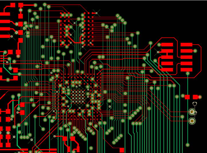
In the realm of multilayer printed circuit board (PCB) design, via technology plays a pivotal role in ensuring the functionality and reliability of complex electronic systems. As electronic devices become increasingly sophisticated, the demand for compact and efficient circuit designs has surged, necessitating the use of multilayer PCBs. These intricate structures, composed of multiple layers of conductive and insulating materials, rely heavily on via technology to establish electrical connections between different layers. Understanding the role of via technology in multilayer PCB design is essential for engineers and designers striving to optimize performance and manufacturability.
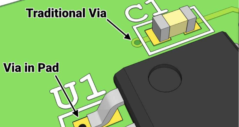
Vias, essentially small holes drilled into the PCB, serve as conduits for electrical signals between the various layers.
They are filled or plated with conductive material, typically copper, to facilitate the transmission of signals. The three primary types of vias used in multilayer PCB design are through-hole vias, blind vias, and buried vias. Each type serves a distinct purpose and is selected based on the specific requirements of the design.
Through-hole vias are the most traditional form of via technology, extending from the top to the bottom layer of the PCB.
They are relatively easy to manufacture and provide robust mechanical support, making them suitable for applications where durability is paramount. However, their use can be limited in high-density designs due to the space they occupy on each layer. To address this limitation, blind and buried vias are employed.
Blind vias connect an outer layer to one or more inner layers without passing through the entire board.
This allows for more efficient use of space, as they do not occupy area on all layers. Buried vias, on the other hand, are located entirely within the inner layers of the PCB, invisible from the outer surfaces. These vias are particularly advantageous in high-density designs, as they free up valuable surface area for additional components and routing.
The selection of via technology is influenced by several factors, including the complexity of the circuit, the number of layers, and the specific electrical requirements.
For instance, high-frequency applications may necessitate the use of microvias, a subset of blind and buried vias, which are smaller in diameter and offer reduced parasitic inductance and capacitance. This is crucial for maintaining signal integrity and minimizing electromagnetic interference.
Moreover, the choice of via technology impacts the manufacturability and cost of the PCB. While through-hole vias are generally more cost-effective, the use of blind and buried vias can increase production complexity and expense. Therefore, designers must carefully balance performance requirements with budgetary constraints.
In addition to their electrical function, vias also play a role in thermal management.
As electronic components generate heat during operation, vias can be used to conduct heat away from critical areas, enhancing the overall thermal performance of the PCB. This is particularly important in high-power applications where efficient heat dissipation is crucial to prevent overheating and ensure reliability.
In conclusion, via technology is an indispensable component of multilayer PCB design, providing essential electrical connections and contributing to thermal management. The careful selection and implementation of vias can significantly influence the performance, manufacturability, and cost of a PCB. As electronic devices continue to evolve, the role of via technology will remain a critical consideration for engineers and designers seeking to push the boundaries of innovation.
Challenges And Solutions In Multilayer PCB Manufacturing
The construction of multilayer printed circuit boards (PCBs) presents a unique set of challenges that require innovative solutions to ensure the reliability and functionality of electronic devices. As the demand for more compact and efficient electronic products grows, the complexity of PCB designs has increased, necessitating the development of multilayer PCBs. These PCBs consist of multiple layers of conductive material separated by insulating layers, allowing for more intricate circuit designs and greater component density. However, this complexity introduces several manufacturing challenges that must be addressed to maintain the integrity and performance of the final product.
One of the primary challenges in multilayer PCB manufacturing is ensuring precise alignment of the layers.
Misalignment can lead to short circuits, open circuits, or other defects that compromise the board’s functionality. To address this issue, manufacturers employ advanced alignment techniques and equipment, such as optical alignment systems, which use cameras and sensors to ensure that each layer is accurately positioned before lamination. Additionally, the use of registration holes and pins can help maintain alignment throughout the manufacturing process.
Another significant challenge is the management of thermal expansion and contraction during the manufacturing process.
The different materials used in multilayer PCBs, such as copper and various substrates, have distinct thermal expansion coefficients. This discrepancy can lead to warping or delamination of the layers when subjected to the high temperatures required for processes like soldering and lamination. To mitigate these effects, manufacturers carefully select materials with compatible thermal properties and employ controlled heating and cooling cycles to minimize stress on the board.
The complexity of multilayer PCBs also necessitates advanced drilling techniques to create the necessary vias and through-holes that connect the different layers.
Traditional mechanical drilling methods can be insufficient for the small diameters and high aspect ratios required in modern multilayer designs. As a solution, laser drilling has become increasingly popular due to its precision and ability to create smaller, more accurate holes. This technology allows for the creation of microvias, which are essential for high-density interconnect (HDI) designs.
Furthermore, the increased layer count in multilayer PCBs can lead to challenges in signal integrity and electromagnetic interference (EMI).
As signals travel through the various layers, they can be affected by crosstalk, impedance mismatches, and other issues that degrade performance. To address these concerns, designers employ techniques such as controlled impedance routing, differential signaling, and the use of ground planes to minimize interference and maintain signal quality. Additionally, advanced simulation tools can be used during the design phase to predict and mitigate potential signal integrity issues.
Finally, the inspection and testing of multilayer PCBs pose their own set of challenges.
The complexity and density of these boards make it difficult to visually inspect for defects, necessitating the use of automated optical inspection (AOI) systems and X-ray inspection to detect hidden issues. Electrical testing, such as flying probe and in-circuit testing, is also crucial to ensure that the board functions as intended.
In conclusion, while the construction of multilayer PCBs presents numerous challenges, advancements in technology and manufacturing techniques have provided effective solutions. By addressing issues related to alignment, thermal management, drilling, signal integrity, and inspection, manufacturers can produce reliable and high-performance multilayer PCBs that meet the demands of modern electronic devices. As technology continues to evolve, ongoing innovation in PCB manufacturing will be essential to keep pace with the ever-increasing complexity of electronic designs.