Multilayer pcb cross section
Understanding The Basics Of Multilayer PCB Cross Section
In the realm of modern electronics, the multilayer printed circuit board (PCB) stands as a cornerstone of technological advancement, enabling the compact and efficient design of complex electronic devices. Understanding the basics of a multilayer PCB cross section is essential for those involved in electronics design and manufacturing, as it provides insight into the intricate structure and functionality of these critical components.
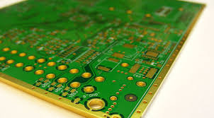
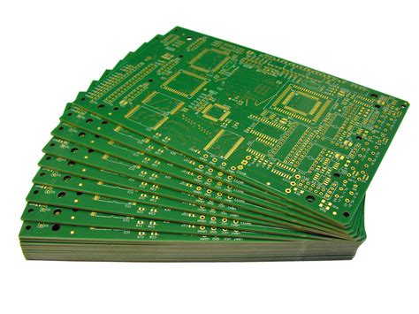
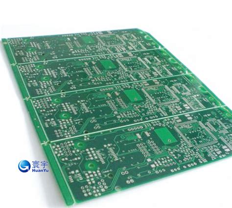
A multilayer PCB is essentially a stack of multiple single-layer PCBs, each separated by insulating material and interconnected through a series of vias. This configuration allows for a higher density of electronic components and interconnections, which is crucial for the miniaturization of electronic devices.
To begin with, the core of a multilayer PCB is typically composed of a substrate material, often made from fiberglass-reinforced epoxy resin, known as FR-4.
This material provides the necessary mechanical support and electrical insulation. On either side of the substrate, copper layers are laminated, forming the conductive pathways for electrical signals. These copper layers are etched to create the desired circuit patterns, which are then interconnected through vias. Vias are small holes drilled through the layers, filled with conductive material, allowing signals to pass between different layers of the PCB.
As we delve deeper into the cross section of a multilayer PCB, it becomes evident that the number of layers can vary significantly, depending on the complexity of the circuit design.
Typically, multilayer PCBs can range from four to as many as fifty or more layers. Each additional layer provides more surface area for routing complex circuits, which is particularly beneficial in applications such as telecommunications, aerospace, and advanced computing systems. The layers are bonded together using a process called lamination, which involves applying heat and pressure to ensure a solid and reliable structure.
Moreover, the design of a multilayer PCB cross section must consider several critical factors to ensure optimal performance.
Signal integrity is paramount, as the close proximity of conductive layers can lead to electromagnetic interference (EMI) and crosstalk between signals. To mitigate these issues, designers often incorporate ground and power planes within the PCB stack-up. These planes act as reference layers, providing a stable voltage level and reducing EMI by shielding signal traces. Additionally, careful attention is paid to the thickness of each layer, as well as the dielectric properties of the insulating material, to maintain the desired electrical characteristics.
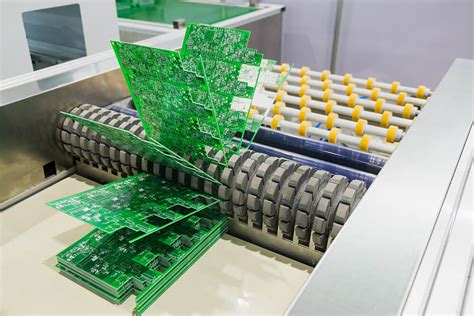
Furthermore, the manufacturing process of multilayer PCBs involves precise control and quality assurance to achieve the desired cross-sectional structure.
Advanced techniques such as laser drilling and automated optical inspection are employed to ensure the accuracy and reliability of the vias and circuit patterns. The complexity of the manufacturing process underscores the importance of understanding the multilayer PCB cross section, as even minor deviations can lead to significant performance issues or failures in the final product.
In conclusion, the multilayer PCB cross section is a fundamental aspect of modern electronics, providing the necessary framework for the development of sophisticated and compact devices. By comprehending the intricacies of its structure, from the substrate material to the arrangement of conductive layers and vias, designers and manufacturers can optimize the performance and reliability of electronic systems. As technology continues to evolve, the role of multilayer PCBs will undoubtedly remain pivotal, driving innovation and enabling the next generation of electronic advancements.
Key Benefits Of Multilayer PCB Cross Section In Modern Electronics
In the rapidly evolving landscape of modern electronics, the multilayer printed circuit board (PCB) cross section has emerged as a pivotal component, offering a multitude of benefits that enhance the functionality and efficiency of electronic devices. As technology continues to advance, the demand for more compact, reliable, and high-performance electronic devices has driven the development and adoption of multilayer PCBs. These sophisticated circuit boards, characterized by their multiple layers of conductive material separated by insulating substrates, provide a range of advantages that are indispensable in contemporary electronic design and manufacturing.
One of the primary benefits of multilayer PCB cross sections is their ability to support high-density interconnections.
As electronic devices become increasingly complex, the need for more connections within a limited space becomes paramount. Multilayer PCBs address this challenge by allowing designers to incorporate multiple layers of circuitry within a single board, thereby maximizing the available space for interconnections. This capability not only facilitates the integration of more components but also enhances the overall performance of the device by reducing the length of interconnecting traces, which in turn minimizes signal loss and electromagnetic interference.
Moreover, the compact nature of multilayer PCBs contributes significantly to the miniaturization of electronic devices.
In an era where portability and space efficiency are highly valued, the ability to pack more functionality into a smaller footprint is a distinct advantage. Multilayer PCBs enable the design of smaller, lighter devices without compromising on performance or reliability. This is particularly beneficial in applications such as smartphones, laptops, and wearable technology, where space is at a premium and every millimeter counts.
In addition to their space-saving attributes, multilayer PCBs offer enhanced electrical performance.
The use of multiple layers allows for the separation of power and ground planes, which helps to reduce noise and improve signal integrity. This separation is crucial in high-speed applications where maintaining signal quality is essential. Furthermore, the ability to incorporate advanced materials and technologies, such as high-frequency laminates and embedded components, within the multilayer structure further enhances the electrical performance of these PCBs, making them suitable for a wide range of demanding applications.
Another significant advantage of multilayer PCB cross sections is their reliability and durability.
The layered construction provides inherent structural strength, which is essential for withstanding the mechanical stresses encountered during manufacturing and operation. Additionally, the use of advanced fabrication techniques and materials ensures that multilayer PCBs can endure harsh environmental conditions, such as extreme temperatures and humidity, making them ideal for use in automotive, aerospace, and industrial applications.
Furthermore, the versatility of multilayer PCBs cannot be overstated.
They can be customized to meet specific design requirements, allowing for the integration of various functionalities within a single board. This flexibility is particularly advantageous in the development of complex systems, where different components must work seamlessly together. By enabling the integration of diverse technologies, multilayer PCBs facilitate the creation of innovative solutions that push the boundaries of what is possible in modern electronics.
In conclusion, the multilayer PCB cross section is a cornerstone of modern electronic design, offering a host of benefits that are crucial for the development of advanced, high-performance devices. From supporting high-density interconnections and enabling miniaturization to enhancing electrical performance and ensuring reliability, multilayer PCBs are indispensable in meeting the demands of today’s technology-driven world. As electronic devices continue to evolve, the role of multilayer PCBs in shaping the future of electronics will undoubtedly remain significant.
Design Considerations For Multilayer PCB Cross Section
In the realm of electronic design, the multilayer printed circuit board (PCB) stands as a cornerstone of modern technology, enabling the compact and efficient assembly of complex electronic circuits. A critical aspect of designing these multilayer PCBs is the cross-sectional configuration, which significantly influences the board’s performance, reliability, and manufacturability. Understanding the intricacies of multilayer PCB cross sections is essential for engineers and designers aiming to optimize their designs for both functionality and cost-effectiveness.
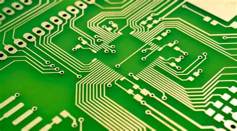
To begin with, the cross section of a multilayer PCB refers to the arrangement and composition of its various layers, including conductive layers, insulating substrates, and any additional materials such as prepregs and solder masks.
The number of layers in a PCB can vary widely, from as few as four to as many as fifty or more, depending on the complexity of the circuit and the specific application requirements. Each layer serves a distinct purpose, with some dedicated to signal routing, others to power distribution, and still others to ground planes, which help in reducing electromagnetic interference and improving signal integrity.
One of the primary considerations in designing a multilayer PCB cross section is the selection of materials.
The choice of substrate material, typically a fiberglass-reinforced epoxy resin known as FR-4, is crucial due to its impact on the board’s thermal and electrical properties. However, for applications requiring higher performance, materials with better thermal conductivity or lower dielectric constants may be selected. Additionally, the thickness of each layer must be carefully determined to balance mechanical strength with electrical performance. Thicker layers can provide better mechanical support but may also increase the board’s overall weight and cost.
Another important factor is the arrangement of the layers themselves.
The stack-up configuration, which refers to the order and orientation of the layers, plays a vital role in determining the PCB’s electrical characteristics. For instance, placing power and ground planes adjacent to each other can create a low-inductance path, which is beneficial for high-speed signal transmission. Moreover, the symmetry of the stack-up is essential to prevent warping during the manufacturing process, which can lead to defects and reduced reliability.
Thermal management is also a critical consideration in multilayer PCB design.
As electronic components become more powerful and compact, the heat generated within a PCB can lead to performance degradation or even failure if not properly managed. Therefore, designers must incorporate thermal vias, heat sinks, and other cooling mechanisms into the cross section to ensure efficient heat dissipation. The choice of materials with high thermal conductivity can further aid in managing heat effectively.
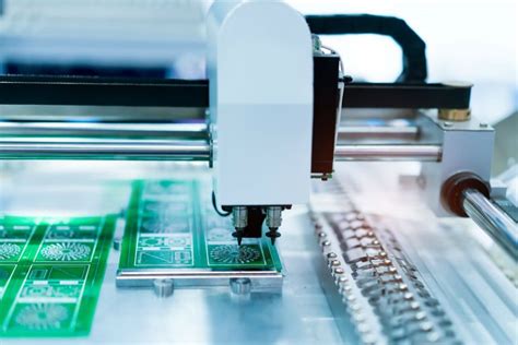
Furthermore, the manufacturability of the PCB must be taken into account during the design phase.
Complex cross sections with numerous layers and intricate routing can pose challenges in fabrication, potentially leading to increased production costs and longer lead times. Designers must work closely with manufacturers to ensure that the proposed design can be produced using available technologies and within budget constraints.
In conclusion, the design of a multilayer PCB cross section is a multifaceted process that requires careful consideration of material selection, layer arrangement, thermal management, and manufacturability. By understanding and addressing these factors, designers can create PCBs that meet the demanding requirements of modern electronic applications, ensuring optimal performance and reliability. As technology continues to advance, the importance of thoughtful and informed PCB design will only grow, underscoring the need for expertise in this critical area.
Common Challenges In Multilayer PCB Cross Section Fabrication
In the realm of electronics manufacturing, multilayer printed circuit boards (PCBs) are indispensable due to their ability to support complex circuitry within a compact form. However, the fabrication of multilayer PCB cross sections presents a myriad of challenges that manufacturers must navigate to ensure functionality and reliability. Understanding these challenges is crucial for optimizing production processes and achieving high-quality outcomes.
One of the primary challenges in multilayer PCB cross section fabrication is maintaining precise layer alignment.
As PCBs become more complex, with an increasing number of layers, the potential for misalignment grows. Misalignment can lead to circuit failures, as electrical connections may not properly align between layers. To mitigate this, manufacturers employ advanced registration systems and alignment techniques. However, even with these technologies, achieving perfect alignment remains a formidable task, requiring meticulous attention to detail and continuous process monitoring.
In addition to alignment issues, the fabrication process must contend with the challenge of ensuring uniform layer thickness.
Variations in layer thickness can result in impedance mismatches, which can adversely affect signal integrity. This is particularly critical in high-frequency applications where even minor discrepancies can lead to significant performance degradation. Manufacturers must carefully control the deposition of materials and employ precise etching techniques to maintain consistent layer thickness across the entire PCB.
Another significant challenge is the management of thermal expansion.
Different materials used in PCB construction, such as copper and various substrates, have distinct coefficients of thermal expansion. During the fabrication process, and later during operation, temperature fluctuations can cause these materials to expand or contract at different rates. This can lead to mechanical stress, delamination, or even cracking of the PCB. To address this, manufacturers often use materials with matched thermal expansion properties and incorporate design features that accommodate thermal stresses.
Furthermore, the increasing demand for miniaturization in electronic devices adds another layer of complexity to multilayer PCB fabrication.
As components become smaller and more densely packed, the margin for error diminishes. This necessitates the use of advanced fabrication techniques, such as laser drilling for microvias, to achieve the necessary precision. However, these techniques can introduce new challenges, such as ensuring the structural integrity of the vias and preventing defects like voids or incomplete fills.
The choice of materials also plays a critical role in the fabrication process.
High-performance applications may require specialized materials that offer superior electrical properties or thermal management capabilities. However, these materials can be more difficult to work with, requiring specialized equipment and processes. Balancing performance requirements with manufacturability is a constant challenge for PCB designers and manufacturers.
Finally, quality control is an overarching challenge that permeates every aspect of multilayer PCB cross section fabrication.
Ensuring that each board meets stringent quality standards requires comprehensive testing and inspection protocols. Techniques such as automated optical inspection (AOI) and X-ray inspection are commonly used to detect defects that may not be visible to the naked eye. However, these methods must be carefully calibrated to avoid false positives or negatives, which can lead to unnecessary rework or undetected failures.
In conclusion, the fabrication of multilayer PCB cross sections is fraught with challenges that require a combination of advanced technology, meticulous process control, and expert knowledge. By understanding and addressing these challenges, manufacturers can produce reliable and high-performance PCBs that meet the demands of modern electronic applications.