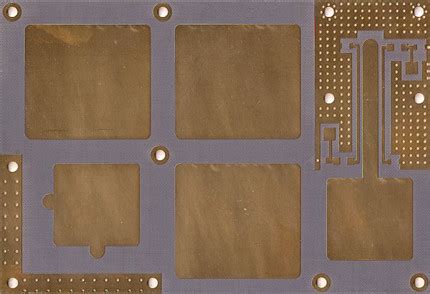
Multilayer pcb diagram
Understanding The Basics Of Multilayer PCB Diagrams
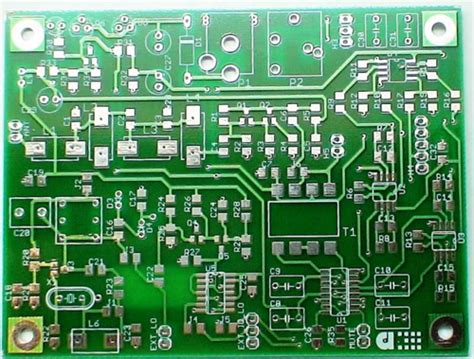
Multilayer printed circuit boards (PCBs) are a cornerstone of modern electronic design, offering enhanced functionality and compactness compared to their single-layer counterparts. Understanding the basics of multilayer PCB diagrams is essential for anyone involved in electronics design or manufacturing. These diagrams serve as blueprints, guiding the intricate process of assembling multiple layers of conductive material and insulating substrates into a cohesive unit. As we delve into the intricacies of these diagrams, it is important to appreciate the complexity and precision they embody.
At the heart of a multilayer PCB diagram is the representation of various layers that make up the board.
Typically, these layers include multiple conductive layers, which are separated by insulating materials known as dielectrics. The conductive layers are usually made of copper and are responsible for carrying electrical signals across the board. The dielectric layers, on the other hand, provide insulation and mechanical support, ensuring that the conductive layers do not short-circuit. In a multilayer PCB diagram, each layer is depicted in a distinct manner, often using different colors or patterns to differentiate between them. This visual distinction is crucial for designers and engineers to accurately interpret the layout and ensure that each layer is correctly aligned during the manufacturing process.
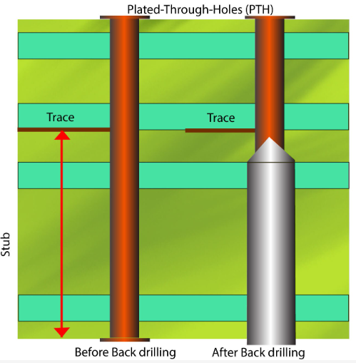
Transitioning from the basic structure, it is essential to understand the role of vias in multilayer PCB diagrams.
Vias are small holes drilled through the board that allow electrical connections between different layers. They are a critical component in multilayer PCBs, enabling complex routing of signals and power. In diagrams, vias are typically represented as small circles or dots, with annotations indicating their function and connection points. Understanding the placement and purpose of vias is vital for ensuring the integrity and performance of the final product.
Moreover, multilayer PCB diagrams also include detailed information about the components and their placement on the board.
Each component is represented by a symbol, accompanied by labels that specify its type, value, and orientation. This information is crucial for the assembly process, as it ensures that each component is placed correctly and functions as intended. Additionally, the diagrams often include a bill of materials (BOM), which lists all the components required for the board, along with their specifications and quantities. This comprehensive documentation is indispensable for both the design and manufacturing stages, facilitating efficient production and quality control.
As we explore further, it is important to consider the significance of signal integrity in multilayer PCB diagrams.
Signal integrity refers to the preservation of signal quality as it travels through the board. In multilayer designs, maintaining signal integrity is particularly challenging due to the increased complexity and density of the circuits. Diagrams play a crucial role in addressing these challenges by providing detailed guidance on trace routing, impedance control, and grounding strategies. By adhering to these guidelines, designers can minimize signal loss and interference, ensuring optimal performance of the final product.
In conclusion, multilayer PCB diagrams are an indispensable tool in the design and manufacturing of modern electronic devices. They provide a comprehensive representation of the board’s structure, components, and connections, facilitating accurate assembly and ensuring high performance. By understanding the basics of these diagrams, designers and engineers can navigate the complexities of multilayer PCB design with confidence, ultimately contributing to the advancement of electronic technology.

Key Components In A Multilayer PCB Diagram
A multilayer printed circuit board (PCB) is a sophisticated and essential component in modern electronic devices, offering enhanced functionality and compactness. Understanding the key components in a multilayer PCB diagram is crucial for engineers and designers who aim to optimize the performance and reliability of electronic systems. At the core of a multilayer PCB is the substrate, typically made from fiberglass-reinforced epoxy resin, which provides structural support and insulation. This substrate forms the foundation upon which multiple layers of conductive material, usually copper, are laminated. The copper layers are etched to create intricate circuit patterns that facilitate electrical connections between components.
Transitioning from the substrate, the next critical component is the dielectric material, which separates the conductive layers.
This insulating layer is vital for preventing electrical interference and ensuring signal integrity. The dielectric material’s properties, such as its dielectric constant and thickness, are carefully selected to match the specific requirements of the PCB’s application. As we delve deeper into the diagram, we encounter vias, which are small holes drilled through the board. Vias serve as conduits for electrical signals, allowing them to traverse between different layers of the PCB. There are several types of vias, including through-hole, blind, and buried vias, each serving distinct purposes based on the design’s complexity and space constraints.
In addition to vias, the multilayer PCB diagram highlights the importance of pads and traces.
Pads are small areas of exposed copper where electronic components are soldered onto the board. These pads are strategically placed to ensure optimal connectivity and mechanical stability. Traces, on the other hand, are narrow pathways of copper that connect different pads and components, forming the circuit’s backbone. The width and thickness of these traces are meticulously calculated to handle the required current without overheating or causing signal loss.
Moreover, the solder mask is another essential component depicted in the multilayer PCB diagram.
This protective layer, typically green, covers the entire board except for the pads, preventing solder bridges and oxidation. The solder mask also enhances the board’s durability by shielding it from environmental factors such as moisture and dust. Complementing the solder mask is the silkscreen layer, which provides valuable information about the board’s layout. This layer includes component labels, reference designators, and other markings that assist in assembly and troubleshooting.
Furthermore, the multilayer PCB diagram often includes ground and power planes, which are large areas of copper dedicated to distributing power and providing a common reference point for signals. These planes play a crucial role in minimizing electromagnetic interference and ensuring stable voltage levels across the board. The careful design of ground and power planes is essential for maintaining the overall performance and reliability of the PCB.
In conclusion, a multilayer PCB diagram is a complex representation of various components that work in harmony to achieve the desired electrical performance. From the substrate and dielectric materials to vias, pads, traces, solder masks, and silkscreens, each element plays a pivotal role in the board’s functionality. Understanding these components and their interactions is fundamental for engineers and designers striving to create efficient and reliable electronic systems. As technology continues to advance, the intricacies of multilayer PCBs will undoubtedly evolve, further underscoring the importance of mastering these foundational concepts.
Designing Efficient Multilayer PCB Diagrams For Complex Circuits
Designing efficient multilayer PCB diagrams for complex circuits is a critical task in the field of electronics engineering, requiring a meticulous approach to ensure functionality, reliability, and manufacturability. As electronic devices become increasingly sophisticated, the demand for compact and efficient circuit designs has led to the widespread adoption of multilayer printed circuit boards (PCBs). These boards, which consist of multiple layers of conductive material separated by insulating layers, offer significant advantages over traditional single-layer designs, including reduced size, improved performance, and enhanced signal integrity.
To begin with, the design process of a multilayer PCB diagram involves several key considerations.
One of the primary factors is the determination of the number of layers required. This decision is influenced by the complexity of the circuit, the number of components, and the need for specific electrical characteristics such as impedance control. Typically, a multilayer PCB can range from four to over twenty layers, with each additional layer providing more routing options and improved electrical performance. However, it is essential to balance the benefits of additional layers with the increased cost and manufacturing complexity they entail.
Once the number of layers is established, the next step is to define the stack-up configuration.
The stack-up refers to the arrangement of conductive and insulating layers within the PCB. A well-designed stack-up is crucial for achieving the desired electrical performance and ensuring the board’s mechanical stability. It also plays a significant role in controlling electromagnetic interference (EMI) and signal integrity. For instance, placing power and ground planes adjacent to each other can create a low-inductance path, which is beneficial for high-speed signal transmission.
In addition to stack-up configuration, careful attention must be paid to the routing of traces on the PCB.
Efficient routing is essential to minimize signal loss, crosstalk, and other potential issues that can arise in complex circuits. Designers often employ techniques such as differential pair routing and controlled impedance routing to maintain signal integrity. Furthermore, the use of vias, which are conductive pathways that connect different layers of the PCB, must be optimized to reduce parasitic inductance and capacitance.
Another critical aspect of designing multilayer PCB diagrams is thermal management.
As electronic components become more densely packed, the risk of overheating increases, potentially leading to component failure. To address this, designers must incorporate thermal vias, heat sinks, and other cooling mechanisms into the PCB design. Additionally, the choice of materials for both the conductive and insulating layers can significantly impact the board’s thermal performance.
Moreover, the integration of design for manufacturability (DFM) principles is essential to ensure that the PCB can be produced efficiently and cost-effectively.
This involves considering factors such as the minimum trace width and spacing, the size and placement of vias, and the overall layout of components. By adhering to DFM guidelines, designers can reduce the likelihood of manufacturing defects and improve the yield of the production process.
In conclusion, designing efficient multilayer PCB diagrams for complex circuits is a multifaceted process that requires a deep understanding of electrical engineering principles and careful consideration of various design factors. By optimizing the number of layers, stack-up configuration, trace routing, thermal management, and manufacturability, engineers can create PCBs that meet the demanding requirements of modern electronic devices. As technology continues to advance, the importance of well-designed multilayer PCBs will only grow, underscoring the need for expertise in this critical area of electronics design.
Common Mistakes To Avoid In Multilayer PCB Diagram Design
Designing a multilayer PCB diagram is a complex task that requires meticulous attention to detail and a deep understanding of electronic design principles. However, even experienced designers can fall prey to common mistakes that can compromise the functionality and reliability of the final product. One of the most frequent errors is inadequate planning of the layer stack-up. The layer stack-up is crucial as it determines the electrical performance, mechanical strength, and thermal management of the PCB. Failing to plan this aspect properly can lead to issues such as signal integrity problems and increased electromagnetic interference. Therefore, it is essential to carefully consider the number of layers, their arrangement, and the materials used.
Another common mistake is neglecting the importance of proper grounding.
A well-designed ground plane is vital for reducing noise and ensuring signal integrity. Designers often overlook the need for a continuous ground plane, which can result in ground loops and increased susceptibility to electromagnetic interference. To avoid this, it is advisable to dedicate at least one layer to a solid ground plane and ensure that it is as unbroken as possible. Additionally, designers should pay attention to the placement of vias, as poorly placed vias can disrupt the ground plane and lead to performance issues.
Furthermore, improper trace routing is a frequent pitfall in multilayer PCB design.
Designers sometimes fail to consider the impact of trace width and spacing on the board’s performance. Traces that are too narrow can lead to increased resistance and potential overheating, while traces that are too close together can cause crosstalk and signal degradation. To mitigate these risks, it is important to adhere to the design rules specified for trace width and spacing, taking into account the current-carrying capacity and the potential for signal interference.
In addition to trace routing, component placement is another area where mistakes are commonly made.
Poor component placement can lead to increased trace lengths, which in turn can cause signal delays and increased inductance. It is crucial to place components in a manner that minimizes trace lengths and facilitates efficient routing. Moreover, designers should consider the thermal implications of component placement, ensuring that heat-generating components are adequately spaced and provided with sufficient cooling mechanisms.
Transitioning to another critical aspect, the failure to perform thorough design rule checks (DRCs) is a mistake that can have significant repercussions.
DRCs are essential for identifying potential design violations that could lead to manufacturing defects or operational failures. Designers should not only rely on automated DRC tools but also conduct manual reviews to catch errors that automated systems might miss. This dual approach helps ensure that the design adheres to all necessary specifications and standards.
Finally, inadequate documentation is a mistake that can complicate the manufacturing process and lead to costly errors.
Comprehensive documentation, including detailed schematics, assembly drawings, and a bill of materials, is essential for ensuring that the PCB is manufactured and assembled correctly. Clear and precise documentation facilitates communication between the designer and the manufacturer, reducing the likelihood of misunderstandings and errors.
In conclusion, while designing a multilayer PCB diagram is a challenging task, being aware of and avoiding these common mistakes can significantly enhance the quality and reliability of the final product. By paying careful attention to layer stack-up, grounding, trace routing, component placement, design rule checks, and documentation, designers can create efficient and effective multilayer PCBs that meet the desired performance criteria.