Multilayer pcb diy
Step-by-Step Guide to Designing Your Own Multilayer PCB
Designing your own multilayer printed circuit board (PCB) can be a rewarding endeavor, offering both a deeper understanding of electronics and the satisfaction of creating a custom solution tailored to your specific needs.
The process, while intricate, can be broken down into manageable steps that ensure a successful outcome. To begin with, it is essential to have a clear understanding of the requirements and specifications of your project. This includes defining the number of layers, the type of components to be used, and the overall dimensions of the PCB.
Once the requirements are established, the next step involves schematic design.
This is where you create a blueprint of your circuit, detailing the connections between various components. Software tools such as Eagle, KiCad, or Altium Designer are invaluable at this stage, providing a user-friendly interface to draw and simulate your circuit. It is crucial to double-check the schematic for errors, as any mistakes here will propagate through the subsequent stages.
Following the schematic design, the layout phase begins.
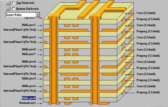
This involves placing the components on the PCB and routing the electrical connections between them. For multilayer PCBs, this step is particularly critical as it requires careful planning to ensure signal integrity and minimize interference. Typically, the inner layers are used for power and ground planes, while the outer layers handle signal routing. Utilizing design rules and constraints within your software can help manage trace widths, spacing, and via sizes, ensuring that the design adheres to manufacturing capabilities.
Transitioning from layout to fabrication, the next step is generating the necessary files for manufacturing.
These files, commonly known as Gerber files, contain all the information needed to produce the PCB, including layer data, drill files, and solder mask information. It is advisable to review these files thoroughly using a Gerber viewer to catch any potential issues before sending them to a manufacturer.
Once the Gerber files are verified, selecting a reliable PCB manufacturer is crucial.
Many manufacturers offer online services where you can upload your files, choose your specifications, and receive a quote. Factors such as turnaround time, cost, and quality should be considered when making your choice. After placing the order, the manufacturer will produce the PCB according to your design specifications.
Upon receiving the fabricated PCB, the next step is assembly.
This involves soldering the components onto the board. Depending on the complexity of your design, this can be done manually or using automated equipment. For DIY projects, manual soldering is often sufficient, though it requires a steady hand and attention to detail to avoid damaging components or creating short circuits.
Finally, testing and validation are critical to ensure that the PCB functions as intended.
This involves powering up the board and checking for correct operation of all circuits. Tools such as multimeters, oscilloscopes, and logic analyzers can be used to diagnose and troubleshoot any issues that arise. It is important to methodically test each section of the PCB, verifying that all connections are correct and that there are no unexpected behaviors.
In conclusion, designing your own multilayer PCB is a complex but achievable task that requires careful planning, attention to detail, and a methodical approach. By following these steps, you can create a custom PCB that meets your specific needs and gain valuable experience in the process. Whether for a personal project or a professional application, the skills and knowledge acquired through this endeavor are invaluable in the field of electronics.
Essential Tools and Materials for DIY Multilayer PCB Projects
Creating a multilayer printed circuit board (PCB) at home can be a rewarding yet challenging endeavor. To ensure success, it is crucial to have the right tools and materials at your disposal. This article will guide you through the essential items needed for a DIY multilayer PCB project, providing a comprehensive understanding of each component’s role in the process.
First and foremost, a high-quality PCB design software is indispensable.
Programs such as Eagle, KiCad, or Altium Designer allow you to create intricate circuit layouts and manage multiple layers effectively. These software tools offer a range of features, including schematic capture, component libraries, and design rule checks, which are vital for ensuring the accuracy and functionality of your PCB design.
Once your design is complete, the next step involves transferring it onto a physical medium.
For this, you will need a laser printer and glossy paper to print the design. The toner transfer method is a popular choice among DIY enthusiasts, as it allows for precise and detailed reproduction of the circuit layout. Additionally, a laminator or a household iron can be used to transfer the toner from the paper to the copper-clad board.
Copper-clad boards are the foundation of any PCB.
These boards come in various sizes and thicknesses, with copper layers on one or both sides. For multilayer PCBs, you will need multiple boards, which will be stacked and bonded together. It is essential to choose high-quality boards to ensure good conductivity and durability.
Etching the copper-clad board is the next critical step.
Ferric chloride or ammonium persulfate are commonly used etching solutions that dissolve the unwanted copper, leaving behind the desired circuit pattern. Safety precautions, such as wearing gloves and working in a well-ventilated area, are necessary when handling these chemicals. A plastic container and a pair of plastic tweezers will also be required to submerge and manipulate the board during the etching process.
After etching, drilling holes for through-hole components and vias is necessary.
A precision drill press or a handheld rotary tool with carbide drill bits will be required for this task. Accurate drilling is crucial for ensuring proper alignment and connectivity between the layers of the PCB.
To create a multilayer PCB, you will need to laminate the individual layers together.
Pre-preg sheets, which are fiberglass materials impregnated with resin, are used to bond the layers. A heat press or a household iron can be employed to apply the necessary pressure and heat to cure the resin, resulting in a solid, unified board.
Soldering is the final step in assembling your PCB. A high-quality soldering iron with a fine tip, along with lead-free solder, is essential for making precise and reliable connections. Flux and desoldering tools, such as a solder wick or a desoldering pump, are also useful for correcting any mistakes.
In addition to these primary tools and materials, several ancillary items can facilitate the process. A multimeter is invaluable for testing continuity and verifying connections. Magnifying tools, such as a jeweler’s loupe or a microscope, can help inspect fine details. Anti-static mats and wrist straps are also recommended to protect sensitive components from electrostatic discharge.
In conclusion, embarking on a DIY multilayer PCB project requires a well-equipped workspace and a thorough understanding of the necessary tools and materials. By investing in high-quality equipment and following proper procedures, you can achieve professional-grade results and bring your electronic designs to life.
Common Mistakes to Avoid When Creating Multilayer PCBs at Home
Creating multilayer printed circuit boards (PCBs) at home can be a rewarding yet challenging endeavor. While the process allows for greater customization and control over the final product, it also presents numerous opportunities for errors. Understanding common mistakes and how to avoid them is crucial for anyone embarking on this intricate task.
One of the most frequent mistakes is inadequate planning.
Multilayer PCBs require meticulous design and layout considerations. Failing to plan the stack-up configuration properly can lead to signal integrity issues and electromagnetic interference. It is essential to determine the number of layers needed and their specific functions before beginning the design process. Utilizing software tools that specialize in PCB design can help streamline this phase, ensuring that each layer is correctly configured and aligned.
Another common error is neglecting thermal management.
Multilayer PCBs often house components that generate significant heat, which can affect performance and longevity. Overlooking the importance of thermal vias and heat sinks can result in overheating and potential failure of the board. Therefore, incorporating adequate thermal management solutions during the design phase is imperative. This includes strategically placing thermal vias and considering the use of materials with high thermal conductivity.
Transitioning from design to fabrication, many DIY enthusiasts underestimate the importance of cleanliness.
Contaminants such as dust, oils, and residues can severely impact the etching process, leading to incomplete or faulty circuits. Ensuring a clean working environment and using appropriate cleaning agents for the PCB material can mitigate these risks. Additionally, wearing gloves and using anti-static mats can further protect the board from contamination and electrostatic discharge.
Moving on to the etching process, improper handling of chemicals is another pitfall.
Etching solutions are often corrosive and require careful handling and disposal. Failing to follow safety protocols can result in personal injury and environmental harm. It is crucial to use protective gear, such as gloves and goggles, and to work in a well-ventilated area. Moreover, understanding the correct concentration and application time for the etching solution can prevent over-etching or under-etching, both of which can compromise the integrity of the PCB.
Soldering is another area where mistakes are commonly made.
Poor soldering techniques can lead to weak joints, bridging, and component damage. Using the correct type of solder and flux, as well as maintaining the appropriate temperature, is vital for achieving reliable connections. Practicing good soldering habits, such as cleaning the soldering iron tip and avoiding excessive heat application, can significantly improve the quality of the final product.
Finally, testing and troubleshooting are often overlooked or inadequately performed.
Skipping this crucial step can result in undetected faults that may only become apparent during operation, leading to costly rework or complete failure. Thoroughly testing each layer and the assembled board for continuity, shorts, and proper functionality is essential. Utilizing tools such as multimeters, oscilloscopes, and specialized testing software can aid in identifying and rectifying issues before they escalate.
In conclusion, creating multilayer PCBs at home is a complex process that demands careful attention to detail and adherence to best practices. By avoiding common mistakes such as inadequate planning, poor thermal management, lack of cleanliness, improper chemical handling, subpar soldering techniques, and insufficient testing, DIY enthusiasts can significantly enhance the quality and reliability of their PCBs. With diligence and precision, the rewarding experience of crafting a functional multilayer PCB is well within reach.
Advanced Techniques for Troubleshooting DIY Multilayer PCBs
When embarking on the intricate task of creating a multilayer printed circuit board (PCB) as a DIY project, it is essential to be equipped with advanced troubleshooting techniques to ensure the functionality and reliability of your design. Multilayer PCBs, with their complex structure and multiple layers of conductive pathways, present unique challenges that require a methodical approach to diagnose and resolve issues effectively.
To begin with, understanding the common problems that can arise in multilayer PCBs is crucial.
Issues such as short circuits, open circuits, and signal integrity problems are prevalent. Short circuits occur when unintended connections form between conductive layers, while open circuits are the result of breaks in the conductive pathways. Signal integrity problems, on the other hand, can manifest as noise, crosstalk, or signal degradation, often due to improper layer stacking or inadequate grounding.
One of the first steps in troubleshooting is to conduct a thorough visual inspection.
Using a magnifying glass or a microscope, examine the PCB for any visible defects such as solder bridges, broken traces, or misaligned components. This initial inspection can often reveal obvious issues that can be corrected with simple rework techniques. However, for more subtle problems, further investigation is necessary.
Electrical testing is a fundamental technique in diagnosing multilayer PCB issues.
Utilizing a multimeter, you can check for continuity and resistance across various points on the board. This helps identify open circuits and short circuits. For more advanced analysis, an oscilloscope can be employed to observe signal waveforms and detect anomalies in signal integrity. By comparing the observed waveforms with expected results, you can pinpoint areas where signal degradation or interference is occurring.
In addition to electrical testing, employing thermal imaging can be highly effective in identifying problematic areas.
Excessive heat generation can indicate short circuits or components operating outside their specified parameters. A thermal camera allows you to visualize temperature variations across the PCB, enabling you to locate hotspots that may require further investigation.
Another advanced technique involves the use of time-domain reflectometry (TDR).
TDR is particularly useful for identifying impedance mismatches and discontinuities in the signal paths. By sending a fast pulse through the PCB and measuring the reflections, you can determine the location and nature of faults within the conductive layers. This method is invaluable for ensuring signal integrity in high-speed digital circuits.
Furthermore, cross-sectional analysis can provide insights into the internal structure of the PCB.
By carefully cutting and polishing a small section of the board, you can examine the layer stack-up, via quality, and overall construction under a microscope. This technique is particularly useful for identifying manufacturing defects that are not visible on the surface.
Incorporating design for testability (DFT) principles during the initial design phase can significantly simplify troubleshooting. By including test points and designing for easy access to critical nodes, you can facilitate more efficient testing and diagnosis. Additionally, using simulation tools to model the PCB’s electrical behavior before fabrication can help identify potential issues early in the design process.
In conclusion, troubleshooting DIY multilayer PCBs requires a combination of visual inspection, electrical testing, thermal imaging, TDR, and cross-sectional analysis. By systematically applying these advanced techniques, you can effectively diagnose and resolve issues, ensuring the functionality and reliability of your multilayer PCB design. As you gain experience and refine your troubleshooting skills, you will be better equipped to tackle the complexities of multilayer PCB projects with confidence.


