Multilayer PCB Manufacturing: A Comprehensive Overview
Introduction
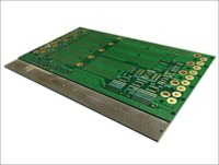
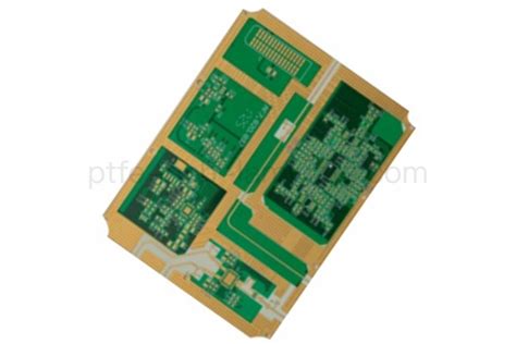
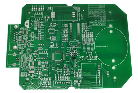
Printed Circuit Boards (PCBs) are the backbone of modern electronics, serving as the foundation for virtually all electronic devices. As technology advances, the demand for more complex and compact electronic systems has led to the development of multilayer PCBs. Unlike single or double-layer PCBs, multilayer PCBs consist of three or more conductive layers, separated by insulating materials, and interconnected through vias. This article provides a comprehensive overview of the multilayer PCB manufacturing process, covering design considerations, materials, fabrication techniques, and quality control.
1. Design Considerations for Multilayer PCBs
The design phase is critical in multilayer PCB manufacturing, as it determines the functionality, reliability, and manufacturability of the final product. Key design considerations include:
1.1 Layer Stackup
The layer stackup defines the arrangement of conductive and insulating layers in the PCB. A typical multilayer PCB stackup includes signal layers, power planes, and ground planes. The stackup must be carefully designed to minimize signal interference, ensure proper impedance control, and manage thermal performance. Common stackup configurations include 4-layer, 6-layer, and 8-layer PCBs, with more layers added as complexity increases.
1.2 Signal Integrity
Signal integrity is a critical concern in multilayer PCBs, especially in high-speed applications. Designers must consider factors such as trace width, spacing, and routing to minimize signal loss, crosstalk, and electromagnetic interference (EMI). Proper impedance matching and the use of differential pairs are essential for maintaining signal integrity.
1.3 Thermal Management
Multilayer PCBs often generate significant heat due to the high density of components and traces. Effective thermal management is essential to prevent overheating and ensure reliable operation. Designers must consider the placement of thermal vias, heat sinks, and copper pours to dissipate heat efficiently.
1.4 Manufacturability
Design for manufacturability (DFM) is a critical aspect of multilayer PCB design. Designers must consider the capabilities and limitations of the manufacturing process, such as minimum trace width, via size, and layer alignment. Adhering to DFM guidelines helps reduce manufacturing defects and improve yield.

2. Materials Used in Multilayer PCB Manufacturing
The choice of materials plays a crucial role in the performance and reliability of multilayer PCBs. Key materials include:
2.1 Substrate Materials
The substrate, or base material, provides the mechanical support for the PCB. Common substrate materials include:
- FR-4: A widely used glass-reinforced epoxy laminate, known for its good electrical insulation, mechanical strength, and cost-effectiveness.
- High-Tg FR-4: A variant of FR-4 with a higher glass transition temperature (Tg), suitable for high-temperature applications.
- Polyimide: A high-performance material with excellent thermal stability, flexibility, and chemical resistance, often used in flexible and rigid-flex PCBs.
- Rogers Materials: High-frequency laminates designed for RF and microwave applications, offering low dielectric loss and stable electrical properties.
2.2 Conductive Materials
Copper is the most commonly used conductive material in PCBs due to its excellent electrical conductivity and cost-effectiveness. The thickness of the copper layer is typically specified in ounces per square foot (oz/ft²), with common thicknesses ranging from 0.5 oz/ft² to 2 oz/ft².
2.3 Insulating Materials
Insulating materials, or prepregs, are used to separate the conductive layers in a multilayer PCB. Prepregs are typically made of woven glass fabric impregnated with resin, which is cured during the lamination process to form a solid insulating layer.
2.4 Solder Mask and Silkscreen
Solder mask is a protective layer applied over the copper traces to prevent solder bridging and protect the PCB from environmental factors. Silkscreen is used to print component labels, logos, and other markings on the PCB surface.

3. Multilayer PCB Fabrication Process
The fabrication of multilayer PCBs is a complex and multi-step process that involves several stages, including:
3.1 Inner Layer Fabrication
The inner layer fabrication process begins with the preparation of the substrate material. Copper foil is laminated onto the substrate, and a photoresist layer is applied. The desired circuit pattern is then transferred onto the photoresist using a photomask and UV light exposure. After developing the photoresist, the exposed copper is etched away, leaving the desired circuit pattern. The remaining photoresist is then stripped, and the inner layers are inspected for defects.
3.2 Layer Alignment and Lamination
Once the inner layers are fabricated, they are aligned and stacked together with prepreg layers in between. The stack is then placed in a lamination press, where heat and pressure are applied to bond the layers together. The lamination process cures the prepreg, forming a solid multilayer structure.
3.3 Drilling
After lamination, holes are drilled through the multilayer stack to create vias and through-holes for component mounting. The drilling process must be precise to ensure proper alignment and avoid damaging the inner layers. Advanced drilling techniques, such as laser drilling, are used for microvias and high-density interconnects (HDIs).
3.4 Plating and Copper Deposition
The drilled holes are then plated with copper to create electrical connections between the layers. This process, known as electroplating, involves depositing a thin layer of copper onto the walls of the holes. The outer layers are also plated with copper to form the outer circuit patterns.
3.5 Outer Layer Fabrication
The outer layer fabrication process is similar to the inner layer process. A photoresist layer is applied to the outer layers, and the desired circuit pattern is transferred using a photomask and UV light exposure. The exposed copper is etched away, and the remaining photoresist is stripped. The outer layers are then inspected for defects.
3.6 Solder Mask Application
A solder mask is applied to the outer layers to protect the copper traces and prevent solder bridging during component assembly. The solder mask is typically applied using a screen printing or photoimaging process, and it is cured to form a durable protective layer.
3.7 Surface Finish
The final step in the fabrication process is the application of a surface finish to the exposed copper areas. Common surface finishes include:
- HASL (Hot Air Solder Leveling): A traditional surface finish that involves coating the copper with a layer of solder and leveling it with hot air.
- ENIG (Electroless Nickel Immersion Gold): A high-quality surface finish that provides excellent solderability and corrosion resistance.
- OSP (Organic Solderability Preservative): A thin, organic coating that protects the copper from oxidation and improves solderability.

4. Quality Control and Testing
Quality control is a critical aspect of multilayer PCB manufacturing to ensure the reliability and performance of the final product. Key quality control measures include:
4.1 Visual Inspection
Visual inspection is performed at various stages of the manufacturing process to identify defects such as misalignment, scratches, and contamination. Automated optical inspection (AOI) systems are often used to detect defects with high precision.
4.2 Electrical Testing
Electrical testing is performed to verify the continuity and functionality of the PCB. Common electrical tests include:
- Continuity Testing: Ensures that all electrical connections are intact and there are no open circuits.
- Insulation Resistance Testing: Measures the resistance between conductive layers to ensure proper insulation.
- Impedance Testing: Verifies that the impedance of the signal traces meets the design specifications.
4.3 X-Ray Inspection
X-ray inspection is used to examine the internal structure of the PCB, including the alignment of vias and the integrity of the inner layers. This non-destructive testing method is particularly useful for detecting defects in high-density interconnects and buried vias.
4.4 Thermal Testing
Thermal testing is performed to evaluate the thermal performance of the PCB under operating conditions. This includes measuring the temperature distribution, thermal resistance, and heat dissipation capabilities of the PCB.
5. Challenges and Future Trends in Multilayer PCB Manufacturing
5.1 Miniaturization and High-Density Interconnects
As electronic devices continue to shrink in size, the demand for miniaturized PCBs with high-density interconnects (HDIs) is increasing. This trend presents challenges in terms of manufacturing precision, material selection, and thermal management. Advanced techniques such as laser drilling, microvia technology, and embedded components are being developed to address these challenges.
5.2 High-Speed and High-Frequency Applications
The proliferation of high-speed and high-frequency applications, such as 5G, IoT, and automotive electronics, is driving the need for PCBs with superior signal integrity and low dielectric loss. This requires the use of advanced materials, such as low-loss laminates, and careful design considerations to minimize signal attenuation and crosstalk.
5.3 Environmental and Regulatory Compliance
Environmental regulations, such as the Restriction of Hazardous Substances (RoHS) directive, are influencing the choice of materials and manufacturing processes in the PCB industry. Manufacturers are increasingly adopting lead-free solders, halogen-free laminates, and eco-friendly manufacturing practices to comply with these regulations.
5.4 Automation and Industry 4.0
The adoption of automation and Industry 4.0 technologies is transforming the PCB manufacturing process. Automated optical inspection (AOI), robotic assembly, and real-time monitoring systems are being integrated into the production line to improve efficiency, reduce defects, and enhance traceability.
Conclusion
Multilayer PCB manufacturing is a complex and highly specialized process that requires careful consideration of design, materials, and fabrication techniques. As the demand for more advanced and compact electronic devices continues to grow, the PCB industry must adapt to new challenges and embrace emerging technologies. By understanding the intricacies of multilayer PCB manufacturing, designers and manufacturers can produce high-quality, reliable PCBs that meet the evolving needs of the electronics industry.


