Multilayer pcb manufacturing machines
Innovations In Multilayer PCB Manufacturing Machines
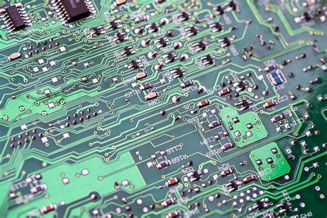
In recent years, the field of electronics has witnessed remarkable advancements, with multilayer printed circuit boards (PCBs) playing a pivotal role in the miniaturization and enhanced functionality of electronic devices. As the demand for more compact and efficient electronic components continues to rise, innovations in multilayer PCB manufacturing machines have become increasingly crucial. These machines are at the forefront of technological progress, enabling the production of complex PCBs with multiple layers, which are essential for modern electronic applications.
One of the most significant innovations in multilayer PCB manufacturing is the development of advanced drilling machines.
These machines are designed to create precise holes, known as vias, which connect different layers of the PCB. Traditional drilling methods often faced limitations in terms of speed and accuracy. However, with the advent of laser drilling technology, manufacturers can now achieve higher precision and faster processing times. Laser drilling not only enhances the quality of the vias but also reduces the risk of damage to the surrounding material, thereby improving the overall reliability of the PCB.
In addition to drilling, the lamination process has also seen substantial improvements.
Lamination is a critical step in multilayer PCB manufacturing, as it involves bonding multiple layers of material together to form a single, cohesive unit. Recent innovations have introduced high-pressure and high-temperature lamination techniques, which ensure a more robust and durable bond between layers. These techniques also allow for the use of advanced materials, such as high-frequency laminates, which are essential for applications requiring high-speed data transmission.
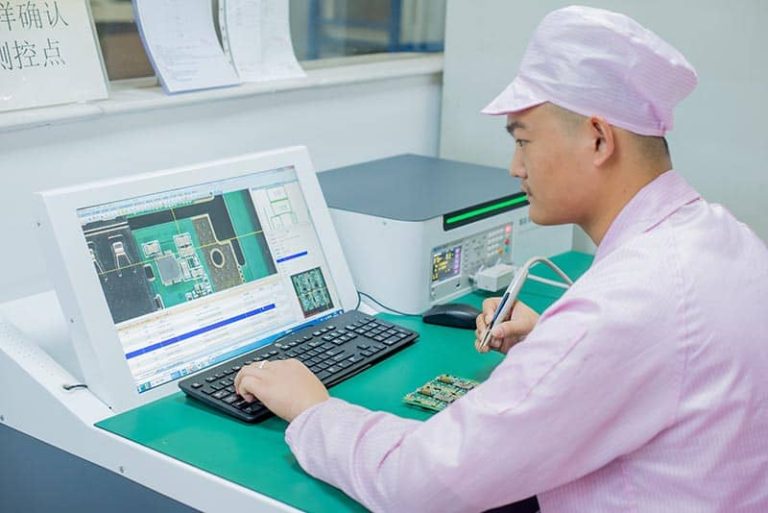
Moreover, the advent of automated optical inspection (AOI) systems has revolutionized the quality control aspect of multilayer PCB manufacturing.
AOI systems utilize high-resolution cameras and sophisticated algorithms to detect defects in PCBs with unparalleled accuracy. This technology not only reduces the likelihood of defective products reaching the market but also enhances the efficiency of the manufacturing process by identifying issues early on. Consequently, manufacturers can implement corrective measures promptly, minimizing waste and improving overall production yield.
Furthermore, the integration of computer-aided design (CAD) and computer-aided manufacturing (CAM) software has streamlined the design and production of multilayer PCBs.
These software solutions enable engineers to create intricate PCB designs with ease, while also facilitating seamless communication between design and manufacturing teams. By automating various aspects of the design process, CAD and CAM software reduce the potential for human error and accelerate the transition from concept to production.
Another noteworthy innovation is the implementation of environmentally friendly manufacturing practices.
As sustainability becomes a growing concern, manufacturers are increasingly adopting green technologies to minimize the environmental impact of PCB production. For instance, water-based cleaning systems and lead-free soldering techniques are being employed to reduce the use of hazardous chemicals. Additionally, energy-efficient machines and processes are being developed to lower the carbon footprint of PCB manufacturing facilities.
In conclusion, the continuous evolution of multilayer PCB manufacturing machines is driving significant advancements in the electronics industry. From laser drilling and high-pressure lamination to automated inspection and eco-friendly practices, these innovations are enhancing the quality, efficiency, and sustainability of PCB production. As technology continues to advance, it is likely that further breakthroughs will emerge, paving the way for even more sophisticated electronic devices in the future.
Key Features To Look For In Multilayer PCB Manufacturing Equipment
When selecting multilayer PCB manufacturing equipment, it is crucial to consider several key features that ensure efficiency, precision, and reliability in the production process. As the demand for complex and compact electronic devices continues to grow, the need for advanced multilayer PCBs has become more pronounced. Therefore, investing in the right manufacturing machines is essential for meeting industry standards and customer expectations.
One of the primary features to consider is the equipment’s capability to handle high-density interconnects (HDI).
As multilayer PCBs often require intricate designs with fine lines and spaces, the machinery must be equipped to manage these complexities. Advanced laser drilling and direct imaging technologies are essential for achieving the precision needed in HDI applications. These technologies allow for the creation of microvias and fine features that are critical in modern PCB designs.
In addition to precision, the speed of the manufacturing process is another vital consideration.
High-speed drilling and routing machines can significantly reduce production time, thereby increasing throughput and efficiency. Automated systems that integrate various stages of the manufacturing process, such as drilling, plating, and etching, can further enhance productivity by minimizing manual intervention and reducing the likelihood of errors.
Moreover, the ability to handle a wide range of materials is an important feature in multilayer PCB manufacturing equipment.
As different applications may require different substrate materials, such as FR-4, polyimide, or Rogers, the machinery should be versatile enough to accommodate these variations. This flexibility ensures that manufacturers can meet diverse customer requirements without the need for multiple specialized machines.
Another critical aspect is the equipment’s capability for quality control and inspection.
Advanced optical inspection systems and automated testing equipment are indispensable for ensuring the integrity and functionality of multilayer PCBs. These systems can detect defects such as misalignments, shorts, and opens, which are crucial for maintaining high-quality standards. Furthermore, real-time monitoring and feedback mechanisms can help in promptly identifying and rectifying issues, thereby reducing waste and rework.
Energy efficiency and environmental considerations are also becoming increasingly important in the selection of manufacturing equipment.
Machines that consume less power and produce minimal waste not only reduce operational costs but also align with sustainable manufacturing practices. Features such as energy-efficient motors, waste recycling systems, and eco-friendly materials contribute to a greener production process.
Additionally, ease of use and maintenance are significant factors to consider.
Equipment with user-friendly interfaces and intuitive controls can reduce the learning curve for operators, leading to smoother operations and fewer errors. Furthermore, machines that are designed for easy maintenance and have readily available spare parts can minimize downtime and extend the equipment’s lifespan.
Finally, scalability and upgradability are essential features for future-proofing the investment in multilayer PCB manufacturing equipment.
As technology evolves and market demands change, the ability to upgrade or expand the machinery’s capabilities can provide a competitive edge. Modular designs and software updates can facilitate this adaptability, ensuring that the equipment remains relevant and efficient over time.
In conclusion, selecting the right multilayer PCB manufacturing equipment involves a careful evaluation of various features that impact precision, speed, versatility, quality control, energy efficiency, ease of use, and scalability. By prioritizing these aspects, manufacturers can enhance their production capabilities and meet the growing demands of the electronics industry.
The Role Of Automation In Multilayer PCB Production
In the rapidly evolving landscape of electronics manufacturing, the production of multilayer printed circuit boards (PCBs) has become increasingly sophisticated. At the heart of this transformation lies the integration of automation, which plays a pivotal role in enhancing the efficiency, precision, and scalability of multilayer PCB production. As the demand for more complex and compact electronic devices grows, manufacturers are compelled to adopt automated solutions to meet these challenges effectively.
To begin with, automation in multilayer PCB manufacturing significantly reduces the margin for error, which is crucial given the intricate nature of these components.
Multilayer PCBs consist of multiple layers of conductive material separated by insulating layers, and any misalignment or defect can lead to circuit failure. Automated machines, equipped with advanced sensors and precision tools, ensure that each layer is accurately aligned and bonded. This precision is particularly important as the number of layers increases, making manual processes not only time-consuming but also prone to human error.
Moreover, automation enhances the speed of production, a critical factor in meeting the high-volume demands of modern electronics markets.
3Automated systems can operate continuously, unlike human workers who require breaks and are subject to fatigue. This capability allows manufacturers to maintain a consistent production flow, thereby reducing lead times and increasing throughput. Consequently, companies can respond more swiftly to market demands and reduce the time-to-market for new products, providing a competitive edge in the fast-paced electronics industry.
In addition to improving accuracy and speed, automation also contributes to cost efficiency in multilayer PCB production.
While the initial investment in automated machinery can be substantial, the long-term savings are significant. Automated systems reduce the need for manual labor, which not only cuts labor costs but also minimizes the risk of costly errors and rework. Furthermore, these machines optimize the use of materials, reducing waste and further lowering production costs. As a result, manufacturers can achieve higher profit margins while offering competitive pricing to their customers.
Transitioning to the environmental impact, automation in PCB manufacturing also supports sustainability efforts.
Automated processes are designed to be more energy-efficient and produce less waste compared to traditional methods. For instance, precision cutting and drilling reduce material wastage, while advanced filtration systems minimize the release of harmful chemicals into the environment. By adopting automated solutions, manufacturers can align with global sustainability goals and meet regulatory requirements, which are becoming increasingly stringent.
Furthermore, the role of automation extends beyond the production line to include quality control and testing.
Automated inspection systems utilize technologies such as machine vision and artificial intelligence to detect defects and ensure that each PCB meets the required specifications. This level of scrutiny is essential for maintaining high-quality standards, especially in industries such as aerospace and medical devices, where reliability is paramount. By integrating automated quality control, manufacturers can ensure consistent product quality and reduce the risk of recalls or failures in the field.
In conclusion, the role of automation in multilayer PCB production is multifaceted, offering benefits that span accuracy, speed, cost efficiency, environmental sustainability, and quality assurance. As technology continues to advance, the capabilities of automated systems will only expand, further solidifying their importance in the manufacturing process. For companies looking to stay competitive in the electronics industry, embracing automation is not just an option but a necessity.
Challenges And Solutions In Multilayer PCB Manufacturing Technology
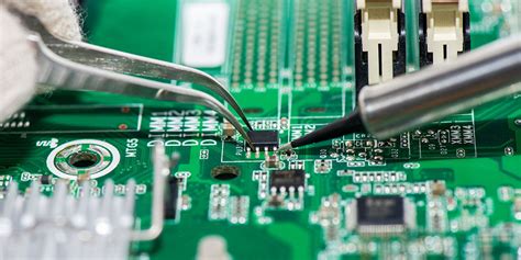
The manufacturing of multilayer printed circuit boards (PCBs) is a complex process that presents numerous challenges, yet it is essential for the advancement of modern electronics. As devices become more compact and require increased functionality, the demand for multilayer PCBs continues to rise. These intricate boards, which consist of multiple layers of conductive material separated by insulating layers, enable the integration of more components in a smaller space. However, the production of such sophisticated boards is fraught with technical difficulties that manufacturers must overcome to ensure quality and reliability.
One of the primary challenges in multilayer PCB manufacturing is maintaining precise alignment of the layers.
Misalignment can lead to circuit failures, rendering the board unusable. To address this issue, manufacturers employ advanced registration systems that use optical alignment techniques. These systems ensure that each layer is accurately positioned relative to the others, minimizing the risk of misalignment. Additionally, the use of automated optical inspection (AOI) machines allows for the early detection of alignment errors, enabling corrective measures to be taken before the board progresses further in the production process.
Another significant challenge is the drilling process, which involves creating vias—small holes that allow electrical connections between layers.
The precision required in drilling is paramount, as any deviation can compromise the board’s functionality. To tackle this, manufacturers utilize high-speed drilling machines equipped with laser technology. These machines offer superior accuracy and can handle the delicate task of drilling microvias, which are essential for high-density interconnect (HDI) PCBs. Moreover, the integration of computer numerical control (CNC) systems in drilling machines enhances precision and repeatability, ensuring consistent quality across batches.
The lamination process, which involves bonding the layers together, also presents challenges.
Achieving uniform pressure and temperature distribution during lamination is crucial to prevent defects such as delamination or air entrapment. To mitigate these issues, manufacturers use advanced lamination presses that offer precise control over pressure and temperature. These machines are often equipped with vacuum systems to eliminate air pockets, ensuring a strong bond between layers. Furthermore, the development of new materials with improved thermal and mechanical properties has contributed to more reliable lamination outcomes.
In addition to these technical challenges, the increasing complexity of multilayer PCBs necessitates sophisticated design and testing processes.
Design software has evolved to accommodate the intricate layouts required for multilayer boards, allowing engineers to simulate and optimize designs before production. This reduces the likelihood of errors and enhances the overall efficiency of the manufacturing process. On the testing front, manufacturers employ a combination of electrical testing and X-ray inspection to verify the integrity of the boards. These methods help identify defects that may not be visible to the naked eye, ensuring that only high-quality boards reach the market.
In conclusion, while the manufacturing of multilayer PCBs presents several challenges, advancements in technology and materials have provided effective solutions.
Through the use of precise alignment systems, high-speed drilling machines, advanced lamination presses, and sophisticated design and testing tools, manufacturers can produce reliable and high-performance multilayer PCBs. As the demand for more compact and capable electronic devices continues to grow, the ongoing development of manufacturing technologies will be crucial in meeting the needs of the industry.