One-Stop PCB Manufacturing and Assembly Services
Key Takeaways
When exploring PCB manufacturing solutions, understanding the end-to-end process helps you make informed decisions. Leading PCB manufacturing companies offer integrated services that cover design validation, material procurement, assembly, and testing—streamlining workflows while minimizing delays.
Tip: Always verify if your provider offers design-for-manufacturability (DFM) analysis. This step prevents costly revisions by aligning your design with production capabilities.
A critical factor in selecting a partner is balancing PCB manufacturing cost with quality. For instance:
| Cost Factor | Impact |
|---|---|
| Material Selection | Affects durability and performance |
| Order Volume | Bulk orders reduce per-unit expenses |
| Testing Protocols | Ensures reliability but adds time |
Modern PCB manufacturing business models prioritize transparency, providing real-time quotes based on your project’s complexity, layer count, and turnaround needs. Advanced techniques like automated optical inspection (AOI) and X-ray testing ensure defects are caught early, reducing long-term risks.
For prototyping, look for providers with 24–48-hour turnaround options—critical for iterative design phases. When scaling to mass production, confirm their capacity to handle high-volume orders without compromising on PCB manufacturing standards.
“Choosing a partner with expertise in rigid-flex and HDI PCBs can future-proof your projects, especially for compact or high-frequency applications.”
By aligning your requirements with a provider’s capabilities, you optimize both timelines and budgets—key to succeeding in competitive markets.
One-Stop PCB Solutions From Design to Production
When navigating the complexities of PCB manufacturing, a seamless design-to-production workflow eliminates bottlenecks and accelerates time-to-market. Leading PCB manufacturing companies integrate every stage—from schematic design validation to final assembly—into a unified process, ensuring design intent translates accurately into functional boards. This approach minimizes errors caused by fragmented workflows, especially when dealing with high-density interconnects (HDIs) or rigid-flex designs.
Understanding PCB manufacturing cost drivers is critical. A turnkey partner like AndwinPCBA optimizes expenses through bulk component sourcing, automated DFM checks, and material substitution analysis without compromising quality. For instance, selecting FR-4 alternatives for non-critical layers or leveraging panelization techniques can reduce material waste by up to 22%.
In the PCB manufacturing business, agility matters. Advanced providers combine rapid prototyping (24-72 hours) with scalable mass production, allowing you to test iterations and transition to full-scale runs seamlessly. Real-time project tracking portals enhance transparency, letting you monitor fabrication milestones, assembly line progress, and testing results concurrently.
Key advantages of integrated solutions include:
- Single-point accountability for design compatibility, eliminating finger-pointing between design houses and fabricators
- Risk mitigation through concurrent engineering reviews during the design phase
- Just-in-time inventory management for components, reducing storage overheads
By aligning with a full-service partner, you bypass the logistical challenges of coordinating multiple vendors—a common pain point in PCB manufacturing. This consolidation not only streamlines communication but also ensures compliance with industry-specific certifications like IPC-A-610 and ISO 13485 for medical devices.
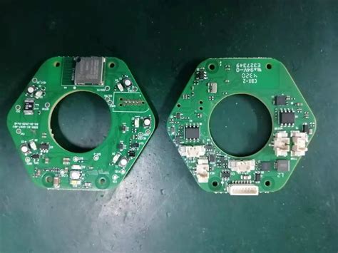
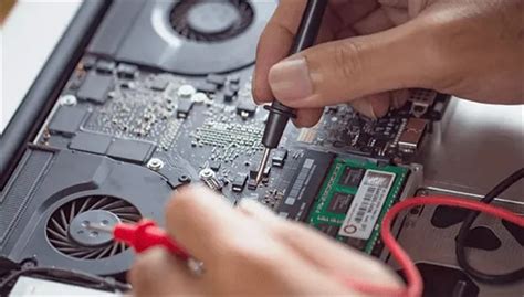
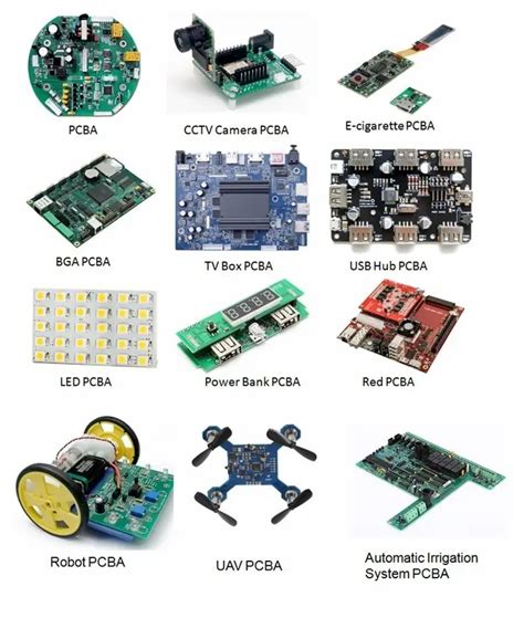
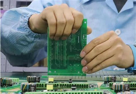
Expert PCB Assembly Techniques and Services
When partnering with PCB manufacturing companies, you gain access to specialized assembly techniques that ensure precision and reliability across every stage of production. Modern PCB manufacturing relies on advanced processes like surface-mount technology (SMT) and through-hole technology (THT), tailored to handle everything from simple single-layer boards to complex rigid-flex or HDI designs. Skilled technicians optimize component placement, solder joint integrity, and thermal management—critical factors that directly influence PCB manufacturing cost and long-term product performance.
A key advantage of integrated services is the seamless coordination between fabrication and assembly. Leading providers synchronize material procurement, automated pick-and-place systems, and rigorous inspection protocols to minimize errors. For instance, automated optical inspection (AOI) and X-ray testing are employed to detect micro-defects, ensuring compliance with industry standards like IPC-A-610. This level of quality control not only reduces rework expenses but also accelerates time-to-market—a vital consideration for scaling your PCB manufacturing business.
Cost efficiency extends beyond technical execution. By consolidating design verification, component sourcing, and assembly under one roof, you eliminate logistical bottlenecks that often inflate budgets. Transparent pricing models further allow you to anticipate PCB manufacturing cost variations based on factors like board complexity, layer count, or finish type. Whether you’re prototyping a high-density interconnect (HDI) design or transitioning to mass production, expert assembly services provide the flexibility to balance speed, quality, and cost predictability.
Leveraging these techniques ensures your project benefits from both technical expertise and operational synergy, positioning your electronics for success in competitive markets.
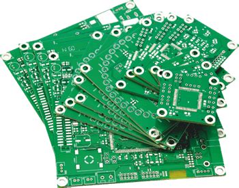
Streamlined PCB Fabrication and Component Sourcing
When developing electronic products, managing PCB manufacturing and component procurement separately often introduces delays and compatibility risks. A streamlined approach integrates fabrication and sourcing into a unified workflow, eliminating bottlenecks that plague traditional methods. Leading PCB manufacturing companies leverage automated design-for-manufacturability (DFM) checks to validate your board files before production begins, reducing costly revisions.
Material selection plays a critical role in controlling PCB manufacturing cost. Reputable providers maintain multi-tiered supplier networks, allowing you to choose between standard FR-4, high-frequency laminates, or metal-core substrates while balancing budget and performance requirements. Advanced procurement systems track global component markets in real time, securing obsolete parts through certified brokers or suggesting form-fit-function equivalents to avoid redesigns.
For businesses scaling their PCB manufacturing business, consolidated logistics prove transformative. Instead of coordinating with fabricators, assemblers, and parts vendors independently, you receive pre-kitted components delivered directly to SMT lines. This just-in-time synchronization minimizes inventory overhead and prevents mismatches between board finishes and solder pastes. Transparent tracking portals provide visibility into every stage – from copper etching to final QA – ensuring your project stays on schedule even during supply chain fluctuations.
By aligning fabrication tolerances with assembly capabilities upfront, this model eliminates the "trial-and-error" phase common in fragmented workflows. Whether producing 10 prototypes or 10,000 finished boards, you maintain control over timelines without compromising on material quality or layer stackup precision.
Advanced SMT/THT Assembly for All PCB Types
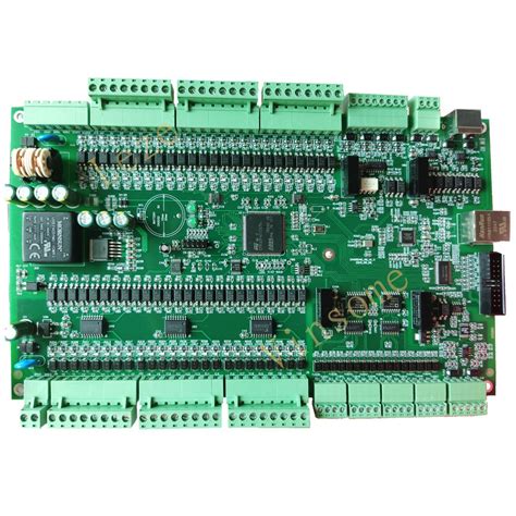
When working with PCB manufacturing companies, the assembly phase determines both functionality and reliability. Modern surface-mount technology (SMT) enables precise placement of micro-components on high-density boards, while through-hole technology (THT) provides robust mechanical bonds for connectors or heavy parts. A skilled PCB manufacturing business leverages both methods to accommodate designs ranging from simple single-layer boards to complex rigid-flex or HDI layouts.
Your project’s PCB manufacturing cost hinges on assembly choices. SMT optimizes space and speed, reducing material waste through automated pick-and-place systems—ideal for miniaturized devices. THT, though slower, ensures durability for industrial applications exposed to vibration or thermal stress. Leading providers integrate automated optical inspection (AOI) post-assembly to verify solder joint integrity, preventing defects before testing phases.
For mixed-technology boards, hybrid assembly lines combine SMT’s efficiency with THT’s strength. This flexibility is critical when prototyping metal-core PCBs for LED systems or multilayer designs for aerospace. By partnering with a full-service PCB manufacturing partner, you avoid fragmented workflows—component sourcing, stencil design, and reflow profiling align under one roof.
Transitioning to volume production? Scalable SMT/THT workflows maintain consistency across batches, whether building 50 prototypes or 10,000 units. Advanced paste printers and nitrogen-reflow ovens prevent oxidation, ensuring repeatable results even for fine-pitch ICs. This end-to-end control minimizes delays, letting you focus on design refinements rather than logistical gaps.
From IoT wearables to automotive controls, the right assembly strategy balances technical requirements with budget realities. By understanding your product’s lifecycle needs, PCB manufacturing experts tailor processes to enhance performance without inflating costs—a cornerstone of competitive electronics development.
Quality Testing in PCB Manufacturing Processes
When partnering with PCB manufacturing companies, understanding their quality assurance protocols becomes critical to ensuring your end product’s reliability. Modern PCB manufacturing workflows integrate multi-stage testing to identify defects early, reducing PCB manufacturing cost overruns caused by rework or failures in the field. Automated optical inspection (AOI) systems, for instance, scan boards at micron-level precision to detect soldering flaws or misalignments, while X-ray inspection verifies hidden connections in high-density interconnect (HDI) designs.
A robust testing strategy also addresses thermal stress and electrical performance. Environmental stress screening (ESS) subjects prototypes to extreme temperatures and humidity, simulating real-world conditions. For functional validation, in-circuit testing (ICT) checks component-level functionality, whereas flying probe tests assess conductivity without physical contact—ideal for fast-turn prototyping. These steps ensure compliance with industry standards like IPC-A-610, which governs acceptance criteria for electronic assemblies.
For businesses managing a PCB manufacturing business, balancing quality and efficiency is non-negotiable. Implementing statistical process control (SPC) tools allows manufacturers to monitor production trends, minimizing variability that could compromise yields. Advanced PCB manufacturing companies further employ design-for-testability (DFT) principles during the design phase, simplifying later-stage inspections.
This approach not only safeguards product integrity but also optimizes PCB manufacturing cost by preventing costly recalls. By prioritizing traceability and data-driven analysis, you gain visibility into potential bottlenecks, ensuring your project transitions smoothly from prototyping to mass production. After all, in an industry where margins hinge on precision, rigorous testing isn’t just a step—it’s the foundation of trust between manufacturer and client.
Fast-Turn PCB Prototyping and Mass Production
When developing electronic products, time-to-market often determines competitive success. Leading PCB manufacturing companies bridge this gap by offering accelerated prototyping cycles—sometimes as fast as 24–48 hours—without compromising precision. This agility stems from integrated workflows where design validation, PCB manufacturing, and functional testing occur in parallel, eliminating traditional bottlenecks.
For startups or enterprises refining designs, managing PCB manufacturing cost during prototyping requires strategic planning. Reputable providers optimize material utilization and leverage bulk purchasing for components, even in small-batch runs. Advanced panelization techniques further reduce waste, ensuring your initial iterations remain budget-friendly. Transitioning to mass production then becomes seamless, as the same team that handled prototypes scales processes using certified high-volume equipment like automated optical inspection (AOI) systems and reel-to-reel assembly lines.
In high-volume scenarios, PCB manufacturing business models prioritize consistency. Multi-stage quality gates—including in-circuit testing (ICT) and X-ray inspection—maintain defect rates below 0.1%. For thermally demanding applications, partnerships with metal-core PCB specialists ensure heat dissipation aligns with industry benchmarks. Crucially, tiered pricing structures in mass production help balance PCB manufacturing cost against order volumes, providing clearer ROI projections.
Whether you require 10 prototypes or 100,000 finished boards, modern PCB manufacturing solutions adapt to both ends of the spectrum. Dual-track services allow concurrent prototyping and production ramp-up, a critical advantage when market windows are narrow. By aligning with partners offering end-to-end traceability and real-time order tracking, you mitigate risks while maintaining velocity from concept to commercialization.
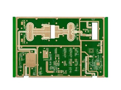
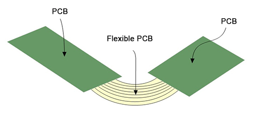
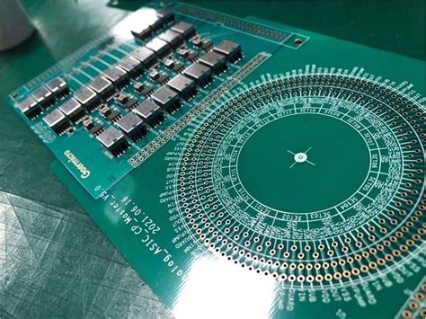
Rigid-Flex and HDI PCB Manufacturing Expertise
When selecting PCB manufacturing companies for complex projects, understanding their capabilities in rigid-flex and HDI PCB manufacturing becomes critical. These advanced technologies cater to applications demanding ultra-high density, space efficiency, or dynamic mechanical performance—think wearable devices, aerospace systems, or implantable medical equipment. Unlike conventional PCBs, rigid-flex designs combine rigid and flexible substrates in a single structure, eliminating connectors and reducing failure points. HDI (High-Density Interconnect) PCBs leverage microvias, finer traces, and sequential lamination to achieve component densities up to 30% higher than traditional boards.
A common concern when engaging in PCB manufacturing business negotiations is balancing technical complexity with PCB manufacturing cost. Reputable suppliers mitigate this through optimized panelization strategies and material selection guidance—for instance, recommending polyimide for high-temperature rigid-flex layers or low-loss laminates for HDI signal integrity. Modern PCB manufacturing workflows now integrate automated impedance control and 3D modeling tools, ensuring designs meet signal integrity thresholds before prototyping.
For projects requiring these specialized techniques, prioritize partners offering end-to-end DFM (Design for Manufacturability) analysis. This includes validating stack-up configurations for rigid-flex bend radii or verifying laser-drilled microvia aspect ratios in HDI layouts. Leading PCB manufacturing companies also provide thermal management solutions, such as embedding copper coins in HDI boards or using adhesiveless flexible materials to enhance heat dissipation.
By aligning your design requirements with a manufacturer’s rigid-flex and HDI PCB manufacturing expertise, you reduce iteration cycles and avoid costly mid-project redesigns. This becomes especially vital when scaling from prototypes to mass production, where consistency in etching tolerance and via plating uniformity directly impacts yield rates. Whether you’re developing compact IoT sensors or multi-layer communication modules, leveraging these advanced capabilities ensures your product meets both performance benchmarks and market timelines.
Cost-Effective Turnkey PCB Services Explained
When managing PCB manufacturing for your projects, balancing quality and affordability is critical. Turnkey solutions simplify this process by consolidating design, fabrication, assembly, and testing under a single provider. This integrated approach eliminates the hassle of coordinating with multiple PCB manufacturing companies, reducing logistical delays and miscommunication risks. By leveraging economies of scale, reputable partners optimize PCB manufacturing cost through bulk material purchasing, automated assembly lines, and streamlined workflows.
A key advantage of turnkey services lies in transparent pricing models. Costs are typically broken down into design validation, PCB manufacturing, component procurement, and quality assurance, allowing you to identify potential savings. For instance, standardizing board sizes or opting for panelization can lower per-unit expenses. Additionally, partnering with a PCB manufacturing business that offers volume discounts ensures scalability, whether you need 10 prototypes or 10,000 production units.
Advanced providers further reduce expenses by maintaining in-house inventories of common components, avoiding third-party markup fees. They also employ design-for-manufacturability (DFM) checks to catch errors early, preventing costly rework. For specialized needs like high-density interconnect (HDI) or rigid-flex boards, experienced vendors apply tailored processes that minimize waste without compromising reliability.
Ultimately, cost-effective turnkey services prioritize end-to-end efficiency—from reducing lead times to automating testing protocols. By aligning your project with a partner that transparently addresses PCB manufacturing cost drivers, you gain predictable budgeting and faster time-to-market, freeing resources to focus on innovation rather than supply chain complexities.
Conclusion
When navigating the complexities of modern electronics production, partnering with experienced PCB manufacturing companies ensures a seamless transition from concept to finished product. By integrating PCB manufacturing with assembly and testing under a single roof, you eliminate logistical bottlenecks while maintaining control over PCB manufacturing cost and timelines. This holistic approach is particularly valuable for businesses balancing precision, scalability, and budget constraints.
A well-structured PCB manufacturing business thrives on optimizing material selection, process automation, and quality assurance protocols. Whether you require low-volume prototypes or high-volume runs, modern providers leverage advanced fabrication techniques to minimize waste and reduce per-unit expenses. Rigid-flex boards, HDI designs, and metal-core PCBs are no longer niche offerings but standardized solutions in comprehensive service portfolios.
Choosing a partner with expertise across the entire value chain—from PCB manufacturing to final assembly—ensures design flaws are identified early, preventing costly revisions. Transparent pricing models demystify PCB manufacturing cost variables like layer count, surface finishes, and testing requirements. For startups and enterprises alike, this clarity transforms capital expenditure planning from a guessing game into a strategic advantage.
Ultimately, the shift toward turnkey solutions reflects the industry’s demand for efficiency without compromising quality. By outsourcing to specialized PCB manufacturing companies, you free internal resources to focus on innovation while relying on proven workflows for consistent, reliable output. As technology evolves, aligning with partners who prioritize adaptability ensures your projects stay ahead in an increasingly competitive landscape.
Frequently Asked Questions
What does a PCB manufacturing company offer in a one-stop service?
A full-service PCB manufacturing provider handles everything from design validation and material procurement to fabrication, assembly, and testing. This eliminates the need to coordinate with multiple vendors, ensuring seamless transitions between stages like component sourcing and SMT assembly.
How is PCB manufacturing cost calculated for custom projects?
Costs depend on factors like board complexity, material type, layer count, and order volume. Most PCB manufacturing companies provide instant quotes after analyzing your design files, balancing quality with budget-friendly options for prototyping or mass production.
Why should I choose a turnkey PCB manufacturing business over multiple vendors?
Managing separate vendors for design, fabrication, and assembly increases risks like communication gaps and delays. A unified PCB manufacturing business streamlines workflows, reduces lead times, and offers cost transparency by bundling services under a single contract.
Can you handle specialized PCB types like rigid-flex or HDI?
Yes. Advanced PCB manufacturing companies support niche requirements, including rigid-flex boards for compact devices and HDI layouts for high-density circuits. They also work with metal-core PCBs for thermal management in industrial applications.
What quality assurance measures are implemented during PCB manufacturing?
Reputable providers use automated optical inspection (AOI), X-ray testing, and functional validation to detect defects. Compliance with standards like IPC-A-600 ensures reliability, especially for mission-critical applications in aerospace or medical devices.
How fast can I expect prototype delivery from a PCB manufacturing service?
Many companies offer 24–48-hour turnaround for prototypes, leveraging in-house facilities to accelerate production. This lets you test designs quickly before committing to large-scale orders.
Ready to Simplify Your PCB Project?
Streamline your workflow with end-to-end solutions tailored to your needs. For a detailed breakdown of services or to request a quote, please click here.