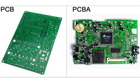
Operational Amplifier (Op-Amp) PCB Design Techniques
Introduction
Operational amplifiers (op-amps) are fundamental components in analog circuit design, widely used in amplification, filtering, signal conditioning, and many other applications. However, even a well-designed op-amp circuit can suffer from performance issues if the printed circuit board (PCB) layout is not optimized. Poor PCB design can lead to noise, oscillations, thermal drift, and signal integrity problems.
This article explores key PCB design techniques for op-amp circuits, covering grounding strategies, component placement, trace routing, power supply decoupling, and thermal considerations to ensure optimal performance.
1. Proper Grounding Techniques
Grounding is critical in op-amp circuits to minimize noise and avoid ground loops.
1.1 Star Grounding
- A star ground configuration connects all ground returns to a single point, reducing ground loops and noise coupling.
- High-current paths (e.g., power supply returns) should be separated from low-level signal grounds.
1.2 Ground Plane Usage
- A solid ground plane reduces impedance and provides a stable reference for signals.
- Avoid splitting ground planes under sensitive analog sections, as this can introduce parasitic inductance.
1.3 Separate Analog and Digital Grounds
- If the PCB includes both analog and digital circuits, keep their grounds separate and connect them at a single point near the power supply.
2. Component Placement Strategies
Proper component placement minimizes parasitic effects and improves signal integrity.
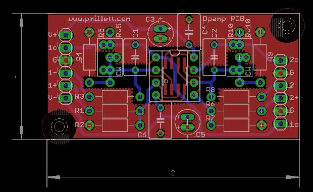
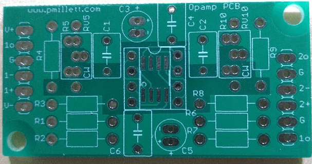
2.1 Keep Feedback Components Close to the Op-Amp
- Place feedback resistors and capacitors as close as possible to the op-amp to minimize stray capacitance and inductance.
- Short traces reduce the risk of unwanted oscillations.
2.2 Minimize High-Impedance Node Lengths
- High-impedance nodes (e.g., inverting input of an op-amp) are sensitive to noise. Keep traces short and avoid running them near noisy signals.
2.3 Position Decoupling Capacitors Near Power Pins
- Place decoupling capacitors (typically 0.1 µF ceramic) as close as possible to the op-amp’s power pins to suppress high-frequency noise.
3. Trace Routing Best Practices
Signal integrity depends heavily on how traces are routed.
3.1 Short and Direct Signal Paths
- Keep input and output traces short to minimize parasitic capacitance and inductance.
- Avoid sharp right-angle turns; use 45° or curved traces to reduce reflections.
3.2 Differential Pair Routing for High-Speed Op-Amps
- For high-speed or precision op-amps, route differential signals symmetrically to maintain signal balance.
3.3 Avoid Crosstalk with Proper Spacing
- Separate high-frequency or high-current traces from sensitive analog signals.
- Use guard rings (grounded copper traces) around high-impedance nodes to shield against interference.
4. Power Supply Decoupling
Proper power supply decoupling ensures stable op-amp operation.
4.1 Use Multiple Decoupling Capacitors
- A combination of bulk (10 µF), medium (1 µF), and high-frequency (0.1 µF) capacitors ensures noise suppression across different frequencies.
- Place the smallest capacitor closest to the op-amp’s power pins.
4.2 Ferrite Beads for Noise Filtering
- In noisy environments, a ferrite bead in series with the power supply can block high-frequency interference.
5. Thermal Considerations
Heat can affect op-amp performance, especially in high-power applications.
5.1 Use Thermal Relief Pads
- For through-hole components, thermal relief pads prevent excessive heat dissipation during soldering.
5.2 Heat Sinking for High-Power Op-Amps
- If the op-amp dissipates significant heat, use a copper pour or dedicated heat sink to improve thermal management.
6. Shielding and EMI Protection
Electromagnetic interference (EMI) can degrade op-amp performance.
6.1 Enclosure Grounding
- Metal enclosures should be grounded to shield against external EMI.
6.2 Guard Traces for Sensitive Signals
- A guard trace (grounded copper surrounding a sensitive trace) reduces leakage currents and capacitive coupling.
7. Testing and Validation
After PCB fabrication, verify performance with:
- Oscilloscope checks for noise and oscillations.
- Frequency response analysis to ensure stability.
- Thermal imaging (if applicable) to detect overheating.
Conclusion
A well-designed PCB is essential for optimal op-amp performance. By following best practices in grounding, component placement, trace routing, decoupling, and thermal management, engineers can minimize noise, avoid oscillations, and ensure signal integrity. Careful attention to these details will lead to robust and reliable analog circuit designs