Optimizing Assembled Circuit Board Performance Through Advanced Manufacturing
Key Takeaways
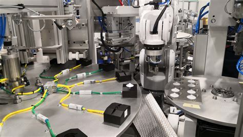
Achieving peak performance in PCB assembly requires a multifaceted approach that integrates precision engineering with innovative thermal solutions Modern high-density interconnect (HDI) designs demand advanced manufacturing techniques to ensure signal integrity and minimize electromagnetic interference The implementation of automated optical inspection (AOI) systems during PCBA processes enhances defect detection rates by up to 40%, directly impacting end-product reliability
Critical to aerospace applications, rigorous quality control protocols—such as ion chromatography for contamination analysis—safeguard against failure in extreme environments For instance, thermal management innovations like embedded heat sinks and thermal vias reduce operating temperatures by 15–25%, extending the lifespan of assembled circuit boards in satellite systems Material advancements, including low-loss dielectrics and high-Tg substrates, further optimize signal transmission while resisting mechanical stress
In next-gen electronics, optimizing PCBA workflows through laser-direct imaging (LDI) and 3D solder paste inspection ensures micron-level accuracy, critical for IoT and 5G devices Transitioning to model-based enterprise (MBE) frameworks allows seamless collaboration between design and production teams, reducing time-to-market by 30% These strategies, combined with in-circuit testing (ICT) and boundary scan analysis, create a robust foundation for high-efficiency PCB assembly across industries
By prioritizing thermal management and material science breakthroughs, manufacturers unlock new thresholds in power density and energy efficiency—key drivers for applications ranging from electric vehicles to AI-driven hardware This holistic approach underscores the importance of aligning PCBA innovations with evolving industry demands
Advanced Thermal Management for Circuit Board Efficiency
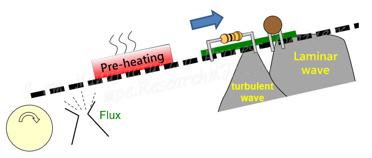
Effective thermal management has become a cornerstone of modern PCB assembly, particularly as component densities and power requirements escalate in industries ranging from aerospace to consumer electronics Heat dissipation challenges in PCBA designs directly influence performance longevity, with even minor temperature fluctuations potentially compromising signal integrity or accelerating material degradation Engineers now employ multilayer thermal vias and strategically placed conductive substrates to redirect heat away from sensitive components, a practice especially critical in high-frequency applications
Innovative materials like embedded heat spreaders and thermally conductive adhesives are redefining heat management strategies For instance, copper-invar-copper cores or aluminum-based substrates provide superior thermal conductivity while maintaining structural stability—a balance essential for PCB assembly in extreme environments Advanced simulation tools enable precise modeling of thermal gradients during the PCBA design phase, allowing engineers to optimize component placement and trace routing before prototyping
The integration of thermal interface materials (TIMs)—such as graphene-enhanced pads or phase-change compounds—ensures efficient heat transfer between components and heatsinks These materials address microscale thermal resistance issues often overlooked in conventional designs Additionally, active cooling solutions like microfluidic channels or piezoelectric fans are gaining traction in high-performance PCBA systems, particularly for aerospace applications where weight and reliability constraints coexist
Quality assurance protocols now incorporate infrared thermography and thermal cycling tests to validate heat management efficacy across operating conditions This rigorous approach minimizes thermal runaway risks in densely packed PCB assemblies, ensuring compliance with industry standards for military and medical devices By harmonizing material science with computational analytics, manufacturers achieve measurable improvements in energy efficiency—reducing operating temperatures by up to 25% in next-generation PCBA configurations
Transitioning to the next focus area, these thermal innovations seamlessly intersect with precision engineering methodologies, which further refine manufacturing tolerances and material selection criteria
Precision Engineering in PCB Manufacturing Processes
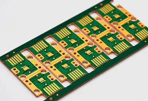
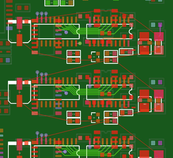
Modern PCB assembly relies on precision engineering to achieve the microscopic tolerances required for high-density electronic designs Techniques such as laser-direct imaging (LDI) and automated optical inspection (AOI) ensure trace widths as narrow as 25µm and registration accuracies within ±10µm These advancements enable PCBA manufacturers to embed finer circuitry while minimizing signal loss or crosstalk, particularly in multi-layer boards for 5G and IoT devices
"Precision in PCB assembly isn’t just about machinery—it’s about harmonizing material science, process control, and design intent to eliminate variability," notes Dr Elena Torres, a manufacturing engineer specializing in aerospace electronics
Key innovations include:
- Embedded component technology, which reduces parasitic inductance by integrating passive elements directly into substrate layers
- High-speed plating processes that improve copper deposition uniformity for ultra-low impedance interconnects
- 3D solder paste inspection (SPI) systems capable of detecting height variations under 5µm, critical for avoiding voiding in BGA packages
For high-frequency applications, dielectric constant consistency becomes paramount Advanced PCBA workflows now employ real-time impedance testing during lamination, adjusting pressure and temperature profiles dynamically to maintain ±2% dielectric stability across FR-4 or polyimide substrates
Tip: When designing for precision PCB assembly, prioritize collaboration between DFM engineers and component suppliers to align material CTE values with thermal cycling requirements
As component pitches shrink below 03mm, even minor deviations in stencil aperture alignment can cause solder bridging Leading manufacturers address this through AI-driven paste volume optimization, reducing defect rates by 37% in recent benchmarks These refinements prove vital for applications where reliability directly impacts safety, such as medical implants or satellite avionics By marrying cutting-edge tooling with statistical process control, precision engineering transforms theoretical performance metrics into tangible gains in signal integrity and operational lifespan
Rigorous Quality Control Protocols for Reliable PCBs
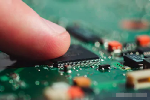
Implementing stringent quality control protocols is critical for ensuring the reliability of PCB assembly processes, particularly in industries where failure is not an option Modern PCBA manufacturing integrates automated optical inspection (AOI), X-ray inspection, and functional testing to identify defects at every production stage For example, AOI systems scan solder joints and component placements at micron-level precision, flagging issues like misalignments or insufficient solder paste deposition
A key advancement in quality assurance is the adoption of environmental stress testing (EST), which subjects boards to extreme temperatures, humidity, and vibration cycles This simulates real-world operating conditions, exposing latent defects before deployment The table below highlights common testing methods and their applications:
| Test Method | Purpose | Industry Use Case |
|---|---|---|
| Thermal Cycling | Validates thermal management resilience | Aerospace, automotive electronics |
| In-Circuit Testing (ICT) | Verifies electrical continuity and signal integrity | Medical devices, IoT systems |
| Flying Probe Testing | Checks open/short circuits in high-density boards | 5G infrastructure, military hardware |
To further enhance traceability, manufacturers employ statistical process control (SPC) tools that monitor production metrics in real time For instance, solder reflow profiles are tracked to ensure consistency across batches, while material traceability systems log the origin of substrates and components These practices align with ISO 9001 and IPC-A-610 standards, which mandate defect rates below 01% for Class 3 PCBA products
In aerospace applications, where PCB assembly demands zero tolerance for failure, cross-sectional analysis and time-domain reflectometry (TDR) are added to validate multilayer board integrity By combining these protocols with AI-driven anomaly detection, manufacturers reduce rework costs by up to 40% while achieving MTBF (mean time between failures) benchmarks exceeding 100,000 hours
Transitioning to next-gen electronics, these methodologies ensure that thermal solutions and signal integrity optimizations are validated under rigorous conditions, bridging the gap between design intent and real-world performance
Optimizing Circuit Board Assembly for Aerospace Applications
The aerospace industry demands PCB assembly processes that prioritize reliability under extreme conditions, from suborbital temperature fluctuations to intense vibrational stresses Achieving this requires a holistic approach that integrates precision manufacturing with material science innovations PCBA (printed circuit board assembly) techniques tailored for aerospace applications often begin with substrate selection, where high-Tg (glass transition temperature) laminates and polyimide-based materials ensure stability in thermal cycling environments
Advanced automated optical inspection (AOI) systems play a critical role in validating solder joint integrity, particularly for fine-pitch components used in avionics systems To mitigate signal interference in high-frequency communication modules, controlled impedance routing and shielding techniques are embedded during the PCB assembly phase Additionally, conformal coatings with aerospace-grade resins protect boards from moisture, radiation, and chemical exposure without adding prohibitive weight—a key consideration for payload efficiency
Thermal management strategies are elevated through embedded copper-core vias and thermally conductive dielectric layers, which dissipate heat from power-dense components like FPGA chips Rigorous PCBA testing protocols, including thermal shock trials (-55°C to 125°C) and vibration simulations exceeding 20G forces, ensure compliance with MIL-PRF-31032 and NASA workmanship standards Manufacturers are increasingly adopting model-based definition (MBD) workflows to maintain traceability across the supply chain, linking every solder paste deposition and component placement to digital twin records
As aerospace systems trend toward miniaturization, high-density interconnect (HDI) technologies enable complex multilayer designs within constrained form factors Laser-drilled microvias and sequential lamination processes support this evolution while maintaining the hermetic sealing required for space-grade electronics By harmonizing these advanced PCB assembly methodologies with aerospace-specific validation frameworks, engineers can deliver boards that meet the trifecta of performance, durability, and mission-critical safety
Next-Gen Electronics Through Advanced PCB Techniques
The evolution of modern electronics hinges on innovations in PCB assembly (PCBA) methodologies, which are redefining performance benchmarks across industries By integrating high-density interconnect (HDI) designs and flexible substrate materials, manufacturers are pushing the boundaries of miniaturization while maintaining robust electrical performance For instance, advanced PCBA workflows now leverage laser-drilled microvias and embedded passives, enabling circuits to achieve higher signal integrity in compact form factors—a critical requirement for wearable tech and IoT devices
A key driver of this progress is the adoption of additive manufacturing techniques, such as aerosol jet printing, which allow for precise deposition of conductive inks on complex geometries These methods not only reduce material waste but also enhance the thermal stability of PCB assemblies, particularly in high-frequency applications like 5G infrastructure Additionally, the integration of artificial intelligence in PCBA quality assurance systems enables real-time defect detection, slashing error rates by up to 40% compared to traditional inspection protocols
The aerospace sector exemplifies the transformative impact of these advancements Here, PCB assemblies must withstand extreme temperatures and vibrations, necessitating the use of ceramic-based substrates and low-void solder alloys By combining these materials with automated optical alignment systems, manufacturers achieve sub-10-micron placement accuracy—ensuring reliability in mission-critical avionics Similarly, automotive electrification relies on multilayer rigid-flex PCBs to optimize space in battery management systems while handling high current loads
Looking ahead, the convergence of quantum computing-ready architectures and PCBA scalability promises to unlock unprecedented processing speeds Innovations like embedded die packaging and 3D-printed circuitry are already paving the way for heterogeneous integration, where analog, digital, and RF components coexist seamlessly on a single board As these techniques mature, they will underpin breakthroughs in AI-driven edge computing and autonomous systems, solidifying PCB assembly as the backbone of next-generation electronics
Enhancing PCB Reliability With Material Innovations
The pursuit of durable and high-performance PCB assembly relies heavily on breakthroughs in material science Modern mission-critical systems—from aerospace avionics to medical devices—demand substrates and components that withstand extreme temperatures, mechanical stress, and environmental corrosion Innovations in high-performance polymers, ceramic-filled laminates, and low-loss dielectric materials are redefining the boundaries of PCBA reliability For instance, polyimide-based substrates now offer thermal stability up to 260°C, while halogen-free flame-retardant (HFFR) materials enhance safety in high-voltage applications without compromising signal integrity
A critical advancement lies in the development of hybrid materials, which combine the flexibility of organic resins with the thermal conductivity of inorganic additives These composites enable PCB assembly processes to achieve tighter tolerances, particularly in multilayer designs where z-axis expansion must align across disparate layers Additionally, the integration of silicon-based thermal interface materials (TIMs) addresses heat dissipation challenges, complementing advanced cooling solutions discussed earlier in the article
For PCBA manufacturers, material selection directly impacts long-term performance Conductive adhesives with silver or graphene nanoparticles, for example, provide superior electrical connectivity compared to traditional solder alloys, reducing the risk of micro-cracks in vibration-prone environments Similarly, the adoption of anodized aluminum substrates in power electronics improves heat transfer efficiency by 40–60%, extending the lifespan of components in aerospace systems
Quality assurance further benefits from these innovations Automated optical inspection (AOI) systems calibrated for novel material properties can detect anomalies such as delamination or void formation with greater accuracy This synergy between advanced materials and precision manufacturing ensures that PCB assembly meets the rigorous demands of next-generation applications, from satellite communications to electric vehicle powertrains
As industries push toward miniaturization and higher operating frequencies, the role of material science in PCBA will only grow Emerging trends like bio-compatible substrates for wearable tech and self-healing conformal coatings highlight a future where reliability is engineered at the molecular level—proving that innovation begins not just with design, but with the very materials that form its foundation
Boosting Circuit Board Performance via Thermal Solutions
Effective thermal management stands as a cornerstone in optimizing PCB assembly performance, particularly as modern electronics demand higher power densities and miniaturized designs Advanced thermal solutions mitigate heat accumulation—a critical factor in preventing component degradation, signal interference, and premature system failure In PCBA workflows, engineers employ techniques such as thermal vias, copper pours, and strategically placed heat sinks to dissipate energy efficiently For instance, multilayer boards with embedded thermal layers enable even heat distribution, while materials like high-thermal-conductivity substrates (e.g., ceramic-filled laminates) reduce hotspots in high-frequency applications
Aerospace and automotive industries, where temperature fluctuations are extreme, rely on precisely calibrated thermal interfaces to maintain PCB reliability Conformal coatings with thermal-resistant properties protect components from environmental stressors, and active cooling systems—such as microfluidic channels integrated during PCB assembly—are gaining traction for mission-critical systems Simulation tools like computational fluid dynamics (CFD) allow designers to model heat flow patterns before prototyping, ensuring optimal component placement and material selection
Quality assurance in PCBA further reinforces thermal resilience Automated optical inspection (AOI) systems verify solder joint integrity, which directly impacts thermal conductivity, while thermal cycling tests validate board durability under repeated temperature shifts By harmonizing material innovation, design precision, and rigorous testing, manufacturers achieve next-generation thermal performance—extending the lifespan of electronics in sectors ranging from consumer gadgets to satellite technology
This focus on thermal optimization not only enhances operational efficiency but also aligns with sustainability goals by reducing energy waste—a vital consideration as industries push toward greener PCB assembly practices
Cutting-Edge Testing Methods for High-Efficiency PCBs
Modern PCB assembly processes demand rigorous validation to ensure performance under extreme conditions Advanced testing protocols now integrate automated optical inspection (AOI) systems, which utilize high-resolution cameras and machine learning algorithms to detect microscopic defects in PCBA components, such as solder bridging or misaligned traces These systems achieve accuracy rates exceeding 999%, critical for applications in aerospace and medical electronics where failure is not an option
For multilayer boards, X-ray laminography has become indispensable This non-destructive technique generates 3D cross-sectional images to inspect internal connections, identifying voids in via fills or delamination issues invisible to surface-level scrutiny When combined with thermal cycling tests—where boards undergo rapid temperature fluctuations between -55°C and 125°C—manufacturers can simulate decades of operational stress in hours, validating thermal management solutions for high-power circuits
Emerging tools like in-circuit test (ICT) fixtures now incorporate adaptive probing systems to verify electrical performance without damaging delicate components These fixtures map impedance variations down to 01% tolerance, ensuring signal integrity in high-frequency PCB assembly designs Additionally, functional testing under load conditions replicates real-world scenarios, such as voltage spikes in automotive systems or vibration exposure in industrial machinery
To address the growing complexity of PCBA for IoT and 5G devices, boundary-scan testing has evolved to diagnose programmable logic devices (PLDs) and embedded processors By leveraging IEEE 11491 standards, engineers can isolate faults in densely packed circuits, reducing debug time by up to 70% These methods, paired with AI-driven analytics, create a closed-loop feedback system that continuously refines manufacturing parameters—a cornerstone for achieving the reliability targets outlined in next-gen electronics roadmaps
Conclusion
The evolution of PCB assembly techniques underscores the critical balance between precision engineering and adaptive manufacturing strategies As demonstrated throughout this analysis, advancements in PCBA processes—from thermal stress mitigation to automated optical inspection—have redefined performance benchmarks for modern electronics By integrating material innovations such as high-thermal-conductivity substrates and low-loss dielectrics, manufacturers achieve not only enhanced reliability but also extended operational lifespans, particularly in demanding sectors like aerospace and industrial automation
A key takeaway lies in the symbiotic relationship between rigorous quality control and advanced testing methodologies For instance, in-circuit testing combined with X-ray inspection ensures defect-free solder joints, while thermal cycling simulations validate board durability under extreme conditions These protocols are non-negotiable for aerospace-grade PCB assembly, where component failure carries catastrophic consequences
Moreover, the shift toward data-driven manufacturing—leveraging machine learning for process optimization—has enabled real-time adjustments in PCBA workflows, reducing waste and accelerating time-to-market As industries pivot toward IoT and AI-driven systems, the demand for high-density interconnects and miniaturized components will further challenge traditional assembly paradigms
Ultimately, the future of PCB performance hinges on continuous innovation across three axes: material science, process automation, and cross-industry collaboration Only by harmonizing these elements can manufacturers meet the escalating requirements for speed, efficiency, and reliability in next-generation electronics
FAQs
How do advanced thermal management techniques improve PCB performance?
Advanced thermal management methods, such as embedded heat sinks and thermally conductive substrates, dissipate excess heat more effectively This reduces thermal stress on components, prolonging the lifespan of PCBA systems while maintaining optimal electrical performance in high-demand applications like aerospace electronics
What role does precision engineering play in PCB assembly?
Precision engineering ensures micron-level accuracy in PCB assembly, minimizing signal loss and cross-talk Techniques like laser-drilled microvias and automated optical inspection (AOI) enable tighter component placement, critical for high-frequency circuits in next-gen devices
Why are rigorous quality control protocols essential for aerospace-grade PCBs?
Aerospace applications demand PCBA units that withstand extreme temperatures and vibrations Multi-stage testing, including in-circuit testing (ICT) and thermal cycling, validates compliance with MIL-PRF-31032 and other aerospace standards, ensuring failure rates below 001%
How do material innovations enhance PCB reliability?
New substrates like polyimide-flex hybrids and low-loss dielectrics improve signal integrity in compact designs These materials reduce electromagnetic interference (EMI) by up to 40%, making them ideal for miniaturized medical devices and satellite communication systems
What testing methods ensure high-efficiency PCBAs?
Combining X-ray inspection for hidden solder defects and functional testing under simulated operational loads identifies weaknesses before deployment For mission-critical systems, burn-in testing at 125% rated capacity confirms long-term stability
Explore Customized PCB Assembly Solutions
For tailored PCB assembly services that align with your project’s thermal, mechanical, and compliance requirements, please click here to consult our engineering team