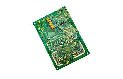
Optimizing HDI PCB Fabrication Costs and Reliability in Design
Key Takeaways
When optimizing HDI PCB fabrication, balancing pcb manufacturing cost with reliability requires strategic planning. Start by evaluating stack-up configurations—each additional layer increases pcb manufacturing business expenses but enhances signal integrity. Work closely with pcb manufacturing companies to identify cost-efficient materials that meet thermal and electrical requirements without over-engineering.
"Prioritize microvia integration early in the design phase. This reduces layer counts while maintaining signal performance, directly lowering pcb manufacturing complexity and costs."
| Factor | Cost Impact | Reliability Benefit |
|---|---|---|
| Layer Reduction | High | Moderate |
| Advanced Microvia Tech | Medium | High |
| Material Selection | Low | High |
Use smart layer count strategies to eliminate unnecessary layers without compromising functionality. For example, combining buried and blind vias can reduce total layers by 20-30% in high-density designs. Always validate your stack-up with pcb manufacturing partners to avoid costly redesigns.
Finally, streamline your design workflow with DFM (Design for Manufacturing) guidelines. Tools like impedance calculators and thermal simulators help prevent reliability issues, ensuring your HDI design aligns with both performance goals and pcb manufacturing cost targets.
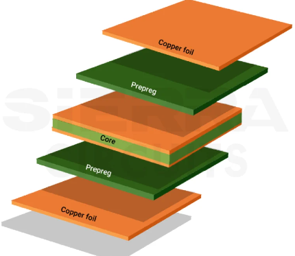
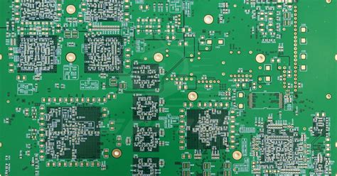
HDI Stack-Up Cost Optimization
Effective HDI stack-up design directly impacts both pcb manufacturing cost and long-term reliability. When planning your layer configuration, prioritize material selection and via architecture to avoid over-engineering. For instance, using hybrid stack-ups—combining standard FR-4 with high-performance substrates in critical areas—can reduce pcb manufacturing expenses by up to 18% while maintaining signal integrity. Collaborate early with pcb manufacturing companies to validate dielectric thickness tolerances, as tighter specs often escalate costs without proportional reliability gains.
A common pitfall is underestimating the role of microvias in layer reduction. By strategically placing blind/buried vias, you can consolidate routing layers, shrinking the overall board thickness and lowering pcb manufacturing business overhead. However, avoid excessive via-in-pad designs unless absolutely necessary, as they require additional laser drilling steps. Tools like impedance calculators help optimize copper weights and trace widths, balancing electrical performance with fabrication feasibility.
Remember, every added layer increases pcb manufacturing cost by 10–15%, so rigorously question whether extra signal planes are justified. For cost-sensitive projects, consider asymmetric stack-ups or staggered via patterns to minimize lamination cycles. By aligning your design choices with production realities, you create a leaner stack-up that accelerates prototyping and scales efficiently for volume runs.
Microvia Reliability in HDI Designs
When designing high-density interconnect (HDI) boards, ensuring microvia reliability directly impacts both performance and pcb manufacturing cost. Aspect ratios and material selection play pivotal roles here—excessive aspect ratios (depth-to-diameter) increase stress risks, while improper dielectric materials can lead to thermal expansion mismatches. To avoid costly rework, you’ll want to collaborate with pcb manufacturing companies that specialize in advanced laser drilling and copper plating techniques, which enhance via wall uniformity and adhesion.
Integrating staggered or stacked microvias? Prioritize simulations to validate their mechanical stability under thermal cycling. This proactive step minimizes field failures, protecting your pcb manufacturing business from reputation damage and warranty claims. Additionally, adopting design-for-manufacturability (DFM) guidelines—like maintaining adequate annular ring widths—helps pcb manufacturing partners optimize yield rates without compromising density goals. Remember, balancing via geometry with process capabilities isn’t just about reliability; it’s a strategic lever to control expenses while meeting stringent HDI performance demands.
Smart Layer Count Strategies
When determining optimal layer counts for HDI PCBs, you need to balance PCB manufacturing cost with performance requirements. Signal integrity and thermal management often drive layer additions, but each new layer increases material expenses and complexity. Start by analyzing your design’s critical functions: high-speed signals may demand dedicated layers, while power planes can often be consolidated. Collaborate early with PCB manufacturing companies to validate your stack-up against their process capabilities—this avoids costly redesigns later.
A 2023 industry analysis found that reducing an 18-layer board to 14 layers (with optimized microvia placement) lowered PCB manufacturing business expenses by 22% without sacrificing reliability. Use simulation tools to identify cross-talk risks and impedance mismatches before finalizing layer counts. For cost-sensitive projects, consider hybrid stacks—mixing standard and high-density layers—to maintain performance while controlling PCB manufacturing budgets. Always prioritize via-in-pad and blind/buried vias in critical areas to minimize layer jumps. By aligning layer strategies with both technical needs and fabrication realities, you create designs that meet reliability benchmarks without inflating production costs.
Streamlining HDI Design Efficiency
To maximize efficiency in HDI PCB manufacturing, you need to prioritize collaboration between design teams and PCB manufacturing companies early in the development cycle. By implementing rule-based design automation tools, you reduce manual errors and accelerate layout iterations, which directly impacts PCB manufacturing cost by minimizing rework. For instance, standardizing via sizes and pad geometries ensures compatibility with your manufacturer’s capabilities, avoiding costly redesigns.
Another critical aspect involves optimizing component placement to minimize signal path lengths. This not only enhances electrical performance but also reduces the need for additional layers—a key factor in controlling PCB manufacturing business expenses. Advanced routing strategies, such as staggered or buried vias, further streamline layer utilization while maintaining signal integrity.
Transitioning to a modular design approach allows reuse of validated circuit blocks across projects, cutting development time by up to 30%. Pair this with real-time DFM (Design for Manufacturability) checks to flag potential issues like insufficient annular rings or copper balancing before prototypes are ordered. Such proactive measures ensure your design aligns with both performance goals and PCB manufacturing budgetary constraints, accelerating time-to-market without compromising reliability.
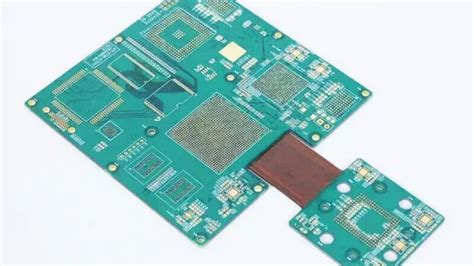
Microvia Integration for Cost Savings
When planning PCB manufacturing for high-density designs, integrating microvias strategically can directly influence PCB manufacturing cost while maintaining reliability. Unlike traditional through-hole vias, microvias—with diameters under 150µm—enable stack-up simplification by replacing multiple staggered vias with fewer, deeper connections. This reduces layer counts and material usage, a critical advantage for PCB manufacturing companies aiming to balance performance and budget.
By adopting laser-drilled microvias, you minimize drilling steps and eliminate unnecessary copper plating, cutting production time by up to 20%. For instance, combining blind/buried microvias with via-in-pad designs shrinks the board footprint, allowing tighter component placement. This efficiency not only lowers PCB manufacturing business overhead but also reduces the risk of signal integrity issues caused by longer traces.
However, collaboration with fabricators early in the design phase is essential. Ensure their capabilities align with your microvia aspect ratios (ideally 1:1 for cost-effective drilling) and material choices. Advanced PCB manufacturing partners can recommend hybrid stack-ups that pair microvias with standard vias in non-critical areas, further optimizing expenses without compromising durability.
Remember: while microvias streamline costs, over-optimizing via density risks fabrication defects. Strike a balance by prioritizing microvias in high-speed or thermal-sensitive zones while using conventional methods elsewhere—a strategy that keeps both reliability and PCB manufacturing cost in check.

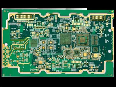
Advanced Stack-Up Planning Techniques
Effective PCB manufacturing begins with strategic stack-up design, where every layer arrangement directly impacts both PCB manufacturing cost and long-term reliability. When planning high-density interconnect (HDI) boards, prioritize signal integrity and thermal management by analyzing impedance control requirements early. Collaborate with PCB manufacturing companies to select dielectric materials that balance performance with budget constraints—for instance, using mid-loss laminates in critical layers while opting for cost-effective substrates in less demanding areas.
A hybrid stack-up approach often proves valuable, combining standard FR-4 with high-speed materials to optimize PCB manufacturing business margins without sacrificing functionality. By reducing the number of sequential lamination cycles through intelligent layer pairing, you can trim production timelines by up to 20%. Advanced simulations help validate designs before prototyping, minimizing costly revisions.
Don’t overlook via structures: staggered or stacked microvias influence layer count and material usage. Tightly coupling power and ground planes improves noise immunity, while adjusting trace widths based on current loads prevents over-engineering. Remember, PCB manufacturing cost escalates with unnecessary layers, so aim for the minimum viable configuration that meets electrical and mechanical specs. Proactive stack-up planning ensures your design aligns with both technical goals and commercial realities.
Balancing HDI Reliability and Budgets
Achieving optimal HDI PCB fabrication outcomes requires balancing reliability imperatives with cost-efficiency goals. While advanced features like stacked microvias enhance performance, they can escalate PCB manufacturing costs if not strategically implemented. Start by evaluating thermal stress thresholds and signal integrity requirements to avoid over-engineering. For instance, using lower-cost resin-coated copper (RCC) materials in non-critical layers maintains mechanical stability without compromising PCB manufacturing business margins.
Collaboration with experienced PCB manufacturing companies ensures design choices align with production capabilities. Tight tolerances or excessive via-in-pad structures might improve reliability but demand specialized equipment, inflating expenses. Instead, adopt asymmetric stack-ups or hybrid via architectures to reduce layer counts while preserving functionality. Simulations tools like 3D EM analysis help identify underutilized features, enabling cost trimming without sacrificing durability.
Finally, consider accelerated life testing (ALT) protocols during prototyping. While this adds upfront PCB manufacturing cost, it minimizes field failures—a critical factor for high-reliability applications. By prioritizing failure mode analysis and leveraging supplier expertise, you optimize both budget and long-term performance, ensuring designs meet market demands without exceeding financial constraints.
Accelerating Time-to-Market with HDI
When integrating HDI PCB fabrication into your product development cycle, balancing speed and precision becomes critical. By collaborating with experienced PCB manufacturing companies, you can leverage design-for-manufacturability (DFM) principles to eliminate costly re-spins. Optimizing PCB manufacturing cost starts with early alignment on stack-up complexity and microvia placement—key factors that influence both production timelines and reliability. For instance, consolidating layers through advanced stack-up planning reduces material waste, while strategically placed microvias minimize signal loss, ensuring your design meets performance benchmarks without unnecessary delays.
To streamline workflows, adopt automated design checks that align with your chosen PCB manufacturing business partner’s capabilities. This prevents mismatches between design intent and fabrication realities, such as improper via fill or insufficient copper balancing. Additionally, modularizing high-density interconnects (HDIs) allows for parallel testing of critical subsystems, slashing validation cycles. Remember, while higher initial PCB manufacturing investments might seem daunting, they often offset long-term risks like field failures or redesign costs. By prioritizing collaborative prototyping and iterative feedback loops, you can compress development timelines while maintaining the rigorous quality standards HDI demands.
Conclusion
Successful HDI PCB fabrication hinges on balancing technical precision with economic efficiency. By implementing advanced stack-up planning and smart layer count strategies, you can reduce PCB manufacturing cost while maintaining signal integrity. Collaborating with experienced PCB manufacturing companies ensures access to cutting-edge microvia technologies, which minimize material waste and assembly errors. Remember that every design choice—from via placement to dielectric selection—impacts both reliability and your PCB manufacturing business’s competitiveness.
To accelerate time-to-market, prioritize designs that align with your manufacturer’s capabilities. This avoids costly redesigns and streamlines production timelines. While optimizing costs, never compromise on critical quality checks—thermal management and impedance control remain non-negotiable for high-density boards. Finally, leverage data-driven insights from past projects to refine future designs, ensuring your PCB manufacturing processes evolve alongside industry standards. By merging innovation with practicality, you secure both performance and profitability in today’s fast-paced electronics landscape.
FAQs
How does advanced stack-up planning affect PCB manufacturing costs?
Strategic layer arrangement minimizes material waste and reduces PCB manufacturing business expenses. By optimizing signal layers and power planes, you avoid unnecessary complexity while maintaining signal integrity.
What role do microvias play in balancing reliability and PCB manufacturing cost?
Properly implemented microvias enhance routing density without compromising structural integrity. This reduces layer counts, lowering PCB manufacturing expenses while improving thermal performance.
How can working with specialized PCB manufacturing companies accelerate time-to-market?
Experienced partners provide design-for-manufacturing (DFM) feedback early, preventing costly revisions. Their expertise in high-density interconnects ensures designs meet both performance goals and budget constraints.
Does reducing layer counts always lower PCB manufacturing cost?
While fewer layers generally reduce material costs, improper reductions risk signal degradation. A balanced approach using smart layer allocation ensures cost savings without sacrificing reliability.
Why is material selection critical for PCB manufacturing business efficiency?
High-performance substrates minimize signal loss and thermal issues, reducing failure rates. Partnering with PCB manufacturing companies that offer material guidance optimizes both cost and long-term reliability.
Ready to Optimize Your HDI PCB Project?
For tailored solutions that align PCB manufacturing cost with reliability, please click here to connect with industry experts. Streamline your design process while maximizing ROI.