Optimizing HDI PCB Layouts for Maximum Density
Key Takeaways
When optimizing HDI PCB design for maximum density, understanding core principles ensures successful implementation. You’ll need to prioritize micro via placement to minimize layer transitions while maintaining signal integrity. Reducing trace widths below conventional thresholds (e.g., 3 mil or less) can free up space, but this requires collaboration with PCB manufacturing companies to verify process capabilities and avoid reliability issues. Compliance with IPC-2226 standards is non-negotiable for high-density layouts, as it governs critical factors like annular ring tolerances and via-in-pad geometries.
Balancing component placement with routing constraints demands iterative adjustments, especially when integrating advanced EDA tools like Altium Designer for real-time design rule checks. For PCB manufacturing cost efficiency, consider how material selection (e.g., low-Dk substrates) impacts both performance and production feasibility. Signal integrity challenges—such as crosstalk in tightly packed traces—can be mitigated through controlled impedance routing and proper grounding strategies.
Finally, aligning your design with PCB manufacturing business capabilities ensures manufacturability. For instance, HDI manufacturing processes often require specialized equipment for laser-drilled vias and sequential lamination. By addressing these elements early, you avoid costly redesigns and achieve ultra-compact layouts without compromising reliability.
Micro Via Strategies for HDI PCBs
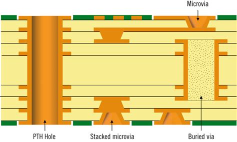
When designing HDI PCBs, optimizing micro via placement is critical for achieving maximum density. You’ll need to balance via geometry, layer transitions, and routing efficiency. Start by prioritizing blind and buried vias over through-hole vias to conserve space, as these structures occupy less vertical real estate. For designs requiring ultra-fine pitch components, consider laser-drilled micro vias (≤100µm diameter) to enable tighter interconnects.
Tip: Stagger micro vias instead of stacking them to reduce stress concentration and improve reliability, as recommended by IPC-2226 guidelines.
A well-planned via strategy directly impacts pcb manufacturing cost and yield. For instance, using too many stacked micro vias increases complexity, which might require specialized processes from pcb manufacturing companies. Here’s a comparison of common via types:
| Via Type | Diameter Range | Layer Transition | Typical Use Case |
|---|---|---|---|
| Through-Hole | 200–300µm | All Layers | Low-density designs |
| Blind | 50–150µm | Outer to Inner | High-speed signal routing |
| Buried | 50–150µm | Inner Layers | Multi-layer HDI stacking |
| Laser Micro Via | ≤100µm | Adjacent Layers | Ultra-compact components |
When collaborating with pcb manufacturing business partners, verify their capability to handle advanced via structures. For example, sequential lamination may be necessary for designs with buried vias, which can affect timelines and pcb manufacturing budgets. Tools like Altium Designer simplify via optimization by automating design rule checks (DRCs) for spacing and aspect ratios, ensuring compliance with IPC-2226.
Remember, thermal management becomes more challenging as via density increases. Use simulation tools to analyze heat dissipation paths, especially in power-heavy sections. By aligning your micro via strategy with both design goals and pcb manufacturing realities, you’ll achieve denser layouts without compromising reliability.
Reducing Trace Width in Dense Layouts
Achieving maximum density in HDI PCB design requires balancing electrical performance with physical constraints. When reducing trace widths below 8 mil, you must account for impedance control and current-carrying capacity to avoid signal degradation or thermal issues. Modern PCB manufacturing processes enable trace widths as narrow as 3 mil, but this demands collaboration with PCB manufacturing companies specializing in high-precision fabrication.
Start by optimizing your design rules in EDA tools like Altium Designer, which supports dynamic width adjustments based on layer-specific requirements. Narrower traces free up routing channels, but ensure spacing adheres to IPC-2226 guidelines to prevent crosstalk. For power traces, calculate minimum widths using current density formulas to avoid overheating—critical in designs where PCB manufacturing cost hinges on material efficiency.
Transitioning to ultra-fine traces also impacts PCB manufacturing business workflows, as tighter tolerances may require laser-direct imaging or advanced etching techniques. Always verify manufacturability through design-for-manufacturing (DFM) checks, particularly when pushing below 5 mil. By strategically reducing trace widths while maintaining signal integrity, you unlock routing space for additional components or shielding structures, directly supporting the goal of ultra-compact layouts.
IPC-2226 Compliance for HDI Design
When designing HDI PCBs, adhering to IPC-2226 standards ensures reliability while pushing density limits. This specification provides critical guidelines for pcb manufacturing processes, particularly for high-density interconnects. By following IPC-2226, you avoid common pitfalls like insufficient annular ring widths or improper microvia aspect ratios, which can escalate pcb manufacturing cost due to rework or yield loss.
A key focus is balancing trace spacing and via structures. For instance, stacked or staggered microvias must meet strict depth-to-diameter ratios to prevent cracking during thermal cycling—a non-negotiable for pcb manufacturing companies specializing in HDI. Tools like Altium Designer simplify compliance checks by automating spacing rules and generating fabrication-ready files, but close collaboration with your pcb manufacturing business partner remains essential. They’ll validate material choices (e.g., low-loss laminates) and ensure designs align with their process capabilities.
Remember, IPC-2226 isn’t just about avoiding failures—it’s about optimizing for scalability. Tightly controlled impedance tolerances and pad geometries enable repeatable performance, even as layer counts increase. By integrating these standards early, you streamline transitions from prototyping to mass production, reducing risks that could derail timelines or budgets.
Component Placement in HDI Optimization
When optimizing HDI PCB layouts, strategic component placement directly impacts both density and performance. Start by grouping high-speed or analog components close to their associated ICs to minimize trace lengths and signal interference. Use 3D stacking techniques to leverage vertical space, but ensure thermal dissipation paths remain unobstructed—collaborating with PCB manufacturing companies early helps validate feasibility and avoid costly redesigns.
Prioritize components requiring fine-pitch connections (e.g., BGAs) near micro vias or buried vias, as this reduces layer transitions and simplifies routing. Avoid clustering heat-sensitive parts near power regulators unless adequate thermal relief is designed. Tools like automated placement algorithms in advanced EDA software can accelerate this process while maintaining IPC-2226 spacing rules.
Balancing PCB manufacturing cost with density goals means avoiding overly complex arrangements that increase fabrication time. For example, placing components symmetrically eases solder mask alignment during PCB manufacturing, improving yield rates. Always verify design rules with your PCB manufacturing business partner to align placement strategies with their process capabilities, ensuring your ultra-compact layout transitions smoothly from design to production.
Altium Designer HDI Layout Techniques
When working with HDI PCB design, Altium Designer provides specialized tools to streamline high-density interconnects while maintaining signal integrity. Start by leveraging its stack-up manager to define precise layer configurations, ensuring optimal micro via placement across blind, buried, and staggered structures. Use the interactive routing feature to minimize trace width reduction errors—critical for avoiding impedance mismatches in ultra-compact layouts.
For IPC-2226 compliance, Altium’s design rule checker (DRC) automates spacing validations between pads and vias, reducing manual verification time. Integrate 3D clearance checks to visualize component interactions in dense areas, a common challenge in pcb manufacturing workflows. When collaborating with pcb manufacturing companies, export Gerber files with embedded layer priorities to clarify fabrication requirements, which helps control pcb manufacturing cost by minimizing rework.
To balance density and manufacturability, prioritize thermal relief settings for high-power components—this prevents heat dissipation issues during assembly. Altium’s flexible design reuse tools also let you replicate proven HDI patterns across projects, accelerating development cycles for pcb manufacturing business clients. Remember, aligning your layout strategy with fabrication capabilities early avoids last-minute adjustments, ensuring your design meets both performance goals and production feasibility.
Signal Integrity in High-Density PCBs
Maintaining signal integrity becomes critical as you push the limits of HDI PCB design to achieve maximum density. With tighter trace spacing and increased layer counts, electromagnetic interference (EMI) and crosstalk risks escalate. To mitigate these, prioritize impedance control by using precisely calibrated trace widths and dielectric materials that match your signal frequency requirements. For high-speed signals, avoid abrupt bends and optimize via placement—staggered or buried microvias reduce parasitic capacitance better than through-hole alternatives.
PCB manufacturing companies often emphasize the importance of ground plane continuity in dense layouts. Split planes or insufficient return paths can degrade signal quality, especially in mixed-signal designs. Simulation tools like HyperLynx or SIProbe in Altium Designer help validate signal integrity before committing to production. When reducing PCB manufacturing cost, balance material selection—low-loss laminates like Megtron 6 improve performance but increase expenses.
Transitioning between layers introduces via stubs, which act as antennas for noise. Back-drilling or using blind vias minimizes this effect, though these techniques add complexity to the PCB manufacturing business. Always collaborate with your fabricator early to align design choices with their process capabilities, ensuring reliable signal paths without exceeding PCB manufacturing tolerances.
HDI Manufacturing for Maximum Density
Achieving ultra-compact designs in HDI PCBs demands precision-driven pcb manufacturing processes that align with advanced design specifications. When partnering with experienced pcb manufacturing companies, you gain access to specialized techniques like sequential lamination and laser-drilled microvias, which are critical for minimizing layer count while maximizing routing density. These processes often involve thinner dielectric materials (≤3 mil) and copper foils (½ oz or lower) to accommodate tighter tolerances, though they can influence pcb manufacturing cost due to increased material and equipment requirements.
To balance cost and performance, prioritize manufacturers capable of handling stacked and staggered vias with sub-100µm diameters, as these structures reduce vertical space consumption. Additionally, registration accuracy (±25µm or better) becomes non-negotiable when dealing with high-density interconnects, as misalignment risks signal degradation. For pcb manufacturing business models targeting IoT or wearables, adopting semi-additive processes (mSAP) can further refine trace widths/spacing to 30/30µm levels, though this requires advanced plating expertise.
When optimizing for density, consider how via-in-pad and buried via strategies impact fabrication complexity. While these methods shrink board area, they may extend lead times unless your manufacturer employs automated optical inspection (AOI) systems for rapid defect detection. Ultimately, aligning your design rules with a pcb manufacturing partner’s capabilities ensures reliable production of high-density layouts without compromising signal integrity or thermal management.
EDA Tools for Compact PCB Designs
When optimizing HDI PCB design, your choice of EDA tools directly impacts achievable density and manufacturability. Modern platforms like Altium Designer and Cadence Allegro provide specialized features for 3D stackup planning and via-in-pad placement, enabling precise routing in ultra-compact layouts. These tools integrate IPC-2226 compliance checks, ensuring designs meet spacing and via-structure guidelines critical for PCB manufacturing reliability.
Advanced simulation modules analyze signal integrity and power distribution early in the design phase, reducing iterations with PCB manufacturing companies. For example, impedance calculators paired with automated DFM (Design for Manufacturability) rules help avoid costly re-spins by aligning trace widths and material choices with PCB manufacturing cost constraints. Tools like Mentor Xpedition offer dynamic length tuning and differential pair routing, essential for maintaining performance in dense boards.
Collaboration features streamline communication with PCB manufacturing business partners, allowing real-time feedback on layer counts or material specifications. By leveraging rigid-flex design modules and embedded component support, you can further shrink footprints while adhering to fabrication limits. Always verify tool outputs against your manufacturer’s capabilities—features like laser-drilled microvias require specific PCB manufacturing tolerances that EDA software must accurately model.
Conclusion
When optimizing HDI PCB layouts, balancing density with reliability requires careful consideration of design choices and PCB manufacturing realities. While strategies like micro via placement and trace width reduction push the boundaries of miniaturization, aligning with PCB manufacturing companies that specialize in high-density designs ensures your vision translates into functional boards. Compliance with IPC-2226 standards remains non-negotiable for avoiding signal integrity issues, but it’s equally critical to factor in PCB manufacturing cost implications early in the design phase. Advanced EDA tools simplify routing in ultra-compact spaces, but their effectiveness depends on collaboration with manufacturers familiar with HDI-specific challenges.
Ultimately, the success of your PCB manufacturing business hinges on harmonizing design innovation with production feasibility. By leveraging stackup optimization and material selection tailored for high-density applications, you minimize rework risks and accelerate time-to-market. Transitioning from design to production smoothly demands clear communication with fabrication partners about tolerances and process capabilities—ensuring your ultra-compact layouts meet both performance goals and PCB manufacturing realities.
FAQs
How do micro vias impact PCB manufacturing costs in HDI designs?
Micro vias enable higher density but require specialized laser drilling, which increases PCB manufacturing cost. However, their precision reduces layer counts, offsetting expenses for ultra-compact designs. Partnering with experienced PCB manufacturing companies ensures optimal via placement for cost-efficiency.
What trace width is feasible while maintaining IPC-2226 compliance?
IPC-2226 permits trace widths as low as 2.5 mils for HDI designs, but signal integrity must be verified. Advanced PCB manufacturing business providers use impedance testing to validate compliance without sacrificing reliability.
Can standard EDA tools handle HDI-specific design rules?
Tools like Altium Designer support HDI constraints, but you’ll need custom design rule checks (DRCs) for blind/buried vias and stacked microvias. Verify capabilities with your PCB manufacturing partner early to avoid redesigns.
How does component placement affect PCB manufacturing yields?
Overcrowding near micro vias or high-density interconnects risks assembly errors. Use 3D modeling in EDA tools to visualize clearances and align with PCB manufacturing companies’ DFM guidelines for maximum yield.
Explore Advanced HDI Manufacturing Solutions
For tailored support in balancing density and manufacturability, please click here to consult experts specializing in high-density PCB manufacturing business solutions.


