Optimizing PCB Design & Assembly for Superior Performance

Key Takeaways
Effective PCB design & assembly relies on harmonizing layout precision, material science, and manufacturing expertise. Key considerations include signal integrity optimization through controlled impedance routing, stackup configuration for high-speed circuits, and thermal management via copper balancing and heatsink integration. For PCBA success, component placement must minimize parasitic effects while aligning with automated assembly workflows.
Material choices—such as high-Tg substrates for thermal resilience or low-loss dielectrics for RF applications—directly impact PCB assembly reliability. Advanced techniques like laser-drilled microvias and sequential lamination enhance density without compromising manufacturability. Cost efficiency emerges through design-for-manufacturing (DFM) principles, including panelization strategies and standardized component libraries.
Critical validation protocols, such as automated optical inspection (AOI) and in-circuit testing (ICT), ensure PCBA performance aligns with design intent. To explore professional implementation frameworks, review industry-leading PCB design methodologies. By integrating these pillars, engineers achieve optimized performance-to-cost ratios across consumer, industrial, and aerospace applications.
PCB Layout Optimization Techniques for Peak Performance
Effective PCB layout optimization forms the foundation of high-performance electronics. By prioritizing signal integrity and minimizing electromagnetic interference (EMI), engineers can ensure stable operation in demanding applications. Key strategies include:
| Design Factor | Optimization Approach | Impact on Performance |
|---|---|---|
| Trace Width/Spacing | Adhere to IPC-2221 standards | Reduces crosstalk & impedance mismatch |
| Layer Stackup | Use dedicated ground/power planes | Enhances EMI shielding |
| Component Placement | Group analog/digital sections separately | Prevents noise coupling |
Tip: Always perform a Design Rule Check (DRC) before finalizing layouts to flag spacing violations or unconnected nets.
For PCB assembly efficiency, maintain a minimum 100-mil clearance between PCBA components and board edges. This prevents mechanical stress during automated soldering. Implementing controlled impedance routing for high-speed signals (e.g., DDR4, PCIe) minimizes reflections, while thermal relief pads improve heat dissipation during reflow processes.
“Optimized layouts reduce PCBA rework costs by up to 40% by avoiding tombstoning or solder bridging,” notes John Miller, Senior PCB Designer at TechCircuits Inc.
Leverage 3D modeling tools to visualize component heights and avoid conflicts in compact designs. When integrating mixed-signal circuits, isolate sensitive analog traces from digital noise sources using guard rings or moats. For multi-layer boards, balance copper distribution across layers to prevent warping during PCB assembly.
Advanced techniques like blind/buried vias enable denser interconnects without compromising manufacturability. Pair these with impedance-matched differential pairs to achieve data rates exceeding 10 Gbps in modern PCBA applications.
Material Selection Strategies in High-Speed PCB Design
Effective PCB assembly begins long before manufacturing—it starts with strategic material selection. In high-speed designs, the choice of substrate and dielectric materials directly impacts signal integrity, thermal stability, and manufacturability. High-frequency applications demand substrates with low dielectric loss (Df) and consistent dielectric constant (Dk) across operating frequencies. Materials like FR-4, polyimide, and specialized laminates such as Rogers 4350B offer varying trade-offs between cost, performance, and thermal resilience. For instance, while FR-4 remains cost-effective for standard pcb design & assembly, high-speed circuits often require low-loss laminates to minimize signal attenuation.
Thermal management is equally critical. Copper weight and thermal conductivity of the substrate influence heat dissipation, which affects both component longevity and PCBA reliability. Advanced designs may incorporate metal-core or ceramic-filled substrates to handle elevated temperatures in power-dense applications. Additionally, selecting compatible solder masks and surface finishes—such as ENIG (Electroless Nickel Immersion Gold) or HASL (Hot Air Solder Leveling)—ensures optimal solderability during PCB assembly, reducing defects like delamination or tombstoning.
For deeper insights into material properties and their impact on performance, refer to this comprehensive guide. By aligning material choices with electrical, thermal, and mechanical requirements, engineers can streamline PCBA workflows while achieving robust, high-speed circuit performance.
Advanced PCB Assembly Processes for Reliability
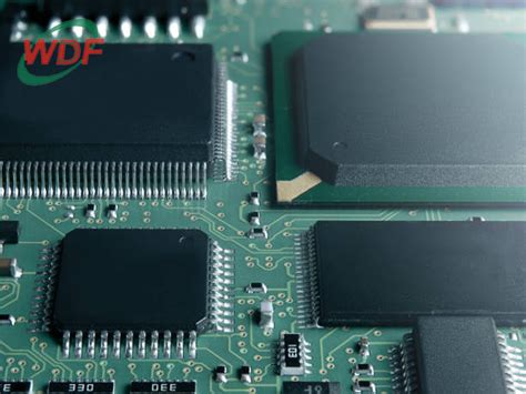
Modern PCB assembly workflows integrate precision engineering with rigorous quality controls to ensure long-term reliability in electronic systems. At the core of reliable PCBA lies automated soldering, which minimizes human error while maintaining consistent joint integrity. Techniques like reflow soldering with optimized thermal profiles prevent voiding and delamination, critical for high-density boards. For mission-critical applications, automated optical inspection (AOI) systems scan solder joints and component placements at micron-level accuracy, flagging defects such as tombstoning or misalignment before final testing.
To enhance durability, manufacturers employ conformal coating processes that protect boards from moisture, dust, and thermal stress. Advanced PCB assembly lines also utilize X-ray inspection to verify internal connections in multilayer designs, addressing hidden flaws like microcracks or via failures. For mixed-technology boards combining SMD and through-hole components, selective soldering offers a hybrid approach, balancing precision with flexibility.
Process consistency is further reinforced through traceability systems, documenting each stage from component sourcing to final PCBA validation. By aligning assembly parameters with design-for-manufacturability (DFM) principles, engineers reduce rework rates and ensure seamless integration with upstream layout optimization and downstream testing protocols.
Cost-Effective Manufacturing Techniques for PCBs
Achieving cost efficiency in PCB assembly requires a balanced approach that prioritizes both quality and affordability. One foundational strategy involves optimizing design-for-manufacturability (DFM) principles, which minimize material waste and reduce production complexities. For instance, standardizing component footprints and avoiding overly dense layouts can lower PCBA costs by streamlining automated placement processes.
Leveraging panelization—grouping multiple boards onto a single substrate—maximizes material utilization and reduces per-unit expenses. However, designers must account for routing and scoring requirements to prevent damage during depanelization. Selecting cost-effective yet reliable materials, such as FR-4 substrates for non-high-frequency applications, further cuts expenses without compromising performance.
Collaboration with PCB assembly partners early in the design phase ensures alignment on tolerances and process capabilities, avoiding costly redesigns. Bulk purchasing of common components and adopting surface-mount technology (SMT) over through-hole parts can yield significant savings, especially for high-volume runs. Additionally, implementing automated optical inspection (AOI) and in-circuit testing (ICT) during PCBA stages reduces post-production defects, minimizing rework costs.
By integrating these strategies, manufacturers can achieve scalable, repeatable processes that deliver high-quality boards while maintaining competitive pricing—a critical advantage in today’s electronics market.
Thermal Management Solutions in PCB Design
Effective thermal management is critical for ensuring the longevity and reliability of modern electronic systems, particularly in high-power or densely packed PCB assembly designs. As component densities increase and operating frequencies rise, managing heat dissipation becomes a cornerstone of successful pcb design & assembly. Key strategies include incorporating thermal vias to transfer heat between layers, optimizing copper pour patterns for improved conductivity, and selecting substrates with low thermal resistance.
In PCBA processes, material selection plays a pivotal role—using metal-core substrates or ceramics can enhance heat dissipation in power electronics. Designers must also balance thermal expansion coefficients between components and the board to prevent mechanical stress during temperature fluctuations. Advanced simulation tools, such as finite element analysis (FEA), enable precise modeling of heat distribution, allowing engineers to identify hotspots before prototyping.
For pcb assembly teams, integrating passive cooling solutions—like strategically placed heat sinks or thermally conductive adhesives—ensures stable operation under load. Additionally, layout optimization techniques, such as spacing high-power components away from sensitive circuits, mitigate cross-thermal interference. Collaborative workflows between design and manufacturing teams are essential to align thermal requirements with PCBA capabilities, ensuring cost-effective production without compromising performance.
Signal Integrity Best Practices for Circuit Boards
Achieving optimal signal integrity in PCB design & assembly requires balancing electromagnetic compatibility, impedance control, and noise reduction. Start by implementing controlled impedance routing for high-speed traces, ensuring minimal signal distortion during PCBA processes. Use ground planes to reduce electromagnetic interference (EMI) and maintain consistent reference voltages, particularly in multilayer designs. Differential pair routing minimizes crosstalk in high-frequency applications, while avoiding sharp angles in traces preserves signal quality during PCB assembly.
Material selection directly impacts performance: low-loss dielectric substrates like Rogers 4350B enhance signal stability for frequencies above 1 GHz. For mixed-signal designs, isolate analog and digital sections with guard traces or split ground planes. MicroArt Services recommends integrating simulation tools like HyperLynx during layout validation to preemptively address reflections or timing mismatches.
In PCBA, ensure surface finishes such as ENIG (Electroless Nickel Immersion Gold) provide reliable solder joints without degrading high-frequency performance. Finally, validate designs with time-domain reflectometry (TDR) testing to confirm impedance consistency across production batches. These strategies, when aligned with rigorous manufacturing techniques, ensure reliable signal transmission in mission-critical applications.
Component Placement Strategies for Efficient Assembly
Effective PCB assembly relies heavily on intelligent component placement to balance performance, manufacturability, and cost. A well-organized layout begins with grouping components by function—power supplies, signal processors, and I/O interfaces should occupy distinct zones to minimize interference. Prioritize placing high-pin-count ICs and heat-sensitive devices first, ensuring adequate spacing for thermal dissipation and PCBA rework access.
Orientation consistency is critical: aligning polarized components (e.g., capacitors, diodes) in the same direction accelerates pick-and-place operations and reduces PCB assembly errors. Additionally, positioning connectors and test points along board edges simplifies post-production validation. For mixed-technology boards, segregate surface-mount (SMD) and through-hole (THT) components to optimize soldering workflows.
Automated assembly efficiency improves when designers adhere to DFM (Design for Manufacturing) guidelines, such as avoiding component shadowing during reflow and maintaining a 0.5mm clearance between parts. Strategic placement of fiducial markers and tooling holes further enhances alignment accuracy in PCBA processes. By integrating these principles, designers ensure smoother transitions to subsequent stages like signal integrity validation and thermal management, while reducing scrap rates and assembly costs.
Testing Protocols for High-Performance PCB Validation
Rigorous testing protocols are critical to ensuring the reliability and performance of PCB assembly (PCBA) in demanding applications. A comprehensive validation strategy begins with electrical continuity checks to identify shorts or open circuits, followed by In-Circuit Testing (ICT) to verify component functionality and parametric values. For high-speed designs, signal integrity analysis using tools like time-domain reflectometry helps detect impedance mismatches or crosstalk that could degrade performance.
Environmental stress testing, including thermal cycling and vibration tests, simulates real-world operating conditions to assess durability. Advanced PCBA validation also incorporates functional testing under simulated loads to confirm board behavior aligns with design specifications. Industry benchmarks recommend combining automated optical inspection (AOI) and X-ray inspection to detect solder joint defects or misaligned components, particularly in fine-pitch or BGA packages.
To maintain alignment with cost-effective manufacturing, test coverage should balance thoroughness with efficiency—leveraging design-for-testability (DFT) principles during layout optimization. This approach not only reduces rework but also strengthens the connection between earlier design phases (such as material selection) and final PCB assembly outcomes, ensuring seamless integration across the product lifecycle.
Conclusion
Achieving optimal performance in PCB design & assembly requires a holistic approach that balances technical precision with manufacturing practicality. By integrating advanced layout optimization with rigorous PCBA processes, engineers can address both electrical performance and production scalability. The interdependence of material selection, thermal management, and signal integrity underscores the need for cross-disciplinary collaboration during the design phase.
Adopting automated assembly workflows in PCB assembly not only enhances repeatability but also minimizes human error, particularly in high-density designs. Meanwhile, cost-effective strategies—such as panelization optimization and standardized component libraries—ensure economic viability without compromising reliability. Post-assembly validation through comprehensive testing protocols remains critical for identifying latent defects and ensuring long-term functionality.
As emerging technologies push the boundaries of miniaturization and speed, aligning PCBA practices with evolving industry standards becomes imperative. By prioritizing proactive design-for-manufacturability (DFM) principles, teams can mitigate risks during prototyping and scale production efficiently. Ultimately, the synergy between meticulous PCB design and precision-driven assembly processes forms the cornerstone of high-performance electronic systems capable of meeting tomorrow’s technological demands.
FAQs
How does design for manufacturability (DFM) impact PCB assembly efficiency?
Adhering to DFM principles ensures compatibility between PCB design and assembly processes, minimizing errors during PCBA. By optimizing pad sizes, component spacing, and layer stack-ups, manufacturers reduce rework and improve yield rates.
What distinguishes PCB fabrication from PCBA in production workflows?
While fabrication focuses on creating the bare board, PCB assembly (PCBA) involves populating the board with components. Advanced PCBA techniques like automated optical inspection (AOI) ensure precise soldering and alignment for high-reliability applications.
How do material choices affect thermal performance in assembled PCBs?
Materials like high-Tg FR-4 or metal-core substrates enhance heat dissipation in PCB assemblies. Proper thermal via placement and copper weight selection during design prevent hotspots, extending the lifespan of PCBA in demanding environments.
What testing methods validate signal integrity in complex PCB assemblies?
Post-assembly tests such as impedance testing and time-domain reflectometry (TDR) verify signal paths. Combined with in-circuit testing (ICT), these protocols ensure PCBA meets performance benchmarks for high-speed applications.
Can cost-effective manufacturing compromise PCB assembly quality?
Strategic decisions like panelization for batch PCB assembly or using standardized components reduce costs without sacrificing reliability. Partnering with certified PCBA providers ensures adherence to ISO and IPC standards while optimizing budgets.
Ready to Optimize Your Next PCB Project?
For tailored PCB assembly solutions that balance performance and cost-efficiency, please click here to explore our expertise in advanced PCBA workflows.