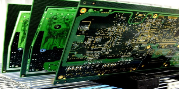
Optimizing PCB Prototype and Assembly Processes
Key Takeaways
Effective optimization of PCB assembly processes begins with understanding critical leverage points across design, fabrication, and testing phases. Implementing design for manufacturability (DFM) principles early reduces rework risks, while selecting standardized components for PCBA lowers procurement delays. To accelerate production cycles, consider adopting just-in-time inventory management and automated pick-and-place systems, which minimize downtime and human error.
Tip: Always validate Gerber files with a design rule check (DRC) before prototyping to avoid costly revisions during PCB assembly.
Balancing speed and precision requires strategic trade-offs. For instance, leveraging rapid prototyping technologies (e.g., 3D printing) shortens lead times but may necessitate stricter post-assembly inspections. Below is a comparison of traditional versus optimized workflows:
| Factor | Traditional Workflow | Optimized Workflow |
|---|---|---|
| Lead Time | 10–14 days | 5–7 days |
| Cost per Unit | $8.50 | $6.20 |
| Defect Rate | 2.1% | 0.7% |
| Scalability | Limited | High |
Quality control remains pivotal—integrate automated optical inspection (AOI) and X-ray testing for PCBA to detect solder joint flaws or component misalignments. Proactively addressing common issues like thermal management inefficiencies or signal integrity problems during prototyping ensures smoother transitions to full-scale production.
By aligning design iterations with PCB assembly capabilities and adopting data-driven process improvements, manufacturers can achieve faster turnaround times without compromising reliability. This foundation sets the stage for exploring advanced innovations in subsequent sections.
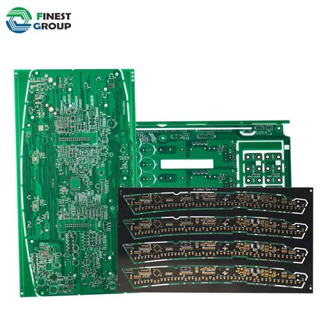
Cost-Efficient PCB Prototyping Tips
Achieving cost efficiency in PCB prototyping begins with optimizing design choices to minimize material waste and rework. Start by leveraging advanced design for manufacturability (DFM) principles, which ensure layouts align with production capabilities. For instance, reducing the number of unique drill sizes or avoiding overly complex trace geometries can lower fabrication costs. Selecting standardized board materials like FR-4 instead of specialty substrates—unless strictly necessary—also contributes to savings.
Collaborating closely with PCBA partners during the prototyping phase helps identify potential assembly challenges early. For example, consolidating surface-mount components on one side of the board simplifies pick-and-place operations, reducing labor time. Additionally, using modular designs or reusable circuitry blocks accelerates iterative testing while trimming development expenses.
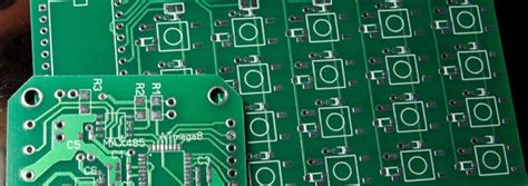
Prototyping techniques such as panelization—grouping multiple designs on a single panel—maximize material utilization and lower per-unit costs. However, ensure adequate spacing between boards to prevent damage during depaneling. For low-volume runs, consider hybrid approaches that combine rapid prototyping methods (e.g., 3D-printed circuits) with traditional PCB assembly workflows to balance speed and affordability.
Finally, validate prototypes through automated optical inspection (AOI) and functional testing to catch defects before scaling production. Early detection of issues like solder bridging or misaligned components avoids costly revisions downstream. By integrating these strategies, manufacturers can maintain precision in PCBA outcomes without compromising budgetary constraints, setting a foundation for seamless transitions to mass production.

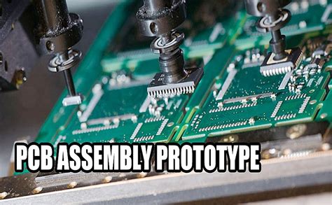
Optimizing PCB Assembly Workflow Efficiency
Effective PCB assembly workflows demand meticulous planning to balance speed and precision. A critical first step involves design-for-manufacturability (DFM) analysis, which identifies potential bottlenecks in PCBA layouts before production begins. Implementing automated pick-and-place systems for surface-mount technology (SMT) components can reduce manual errors by up to 40%, while inline optical inspection (AOI) systems ensure real-time quality validation.
Transitioning to modular workflows allows manufacturers to segment PCB assembly stages—such as solder paste application, component placement, and reflow soldering—into parallel processes. This approach minimizes idle time and accelerates throughput. For instance, integrating just-in-time (JIT) inventory management with automated material handling systems reduces component staging delays by 25–30%.
Collaboration between design and production teams further refines workflow efficiency. By standardizing panelization strategies for multi-board designs, manufacturers optimize material utilization and reduce PCBA cycle times. Additionally, adopting closed-loop feedback systems enables continuous process adjustments, addressing deviations before they escalate. These strategies not only streamline operations but also align with broader goals of cost reduction and quality assurance, ensuring seamless progression to subsequent production phases.
Accelerating PCB Production Cycles Strategically
Strategic acceleration of PCB assembly timelines requires a multi-faceted approach that balances speed with technical rigor. Implementing design for manufacturability (DFM) principles early in the prototyping phase minimizes rework by identifying potential bottlenecks in PCBA workflows. For instance, leveraging automated design validation tools can reduce layout errors by up to 40%, directly shortening iteration cycles.
Critical to this acceleration is the integration of just-in-time (JIT) inventory systems for components, paired with vendor-managed stocking programs. This ensures critical parts like high-density interconnects or specialty substrates are available without overstocking, which can delay prototyping. Additionally, adopting modular PCB assembly workflows—where standardized subassemblies are pre-tested—allows parallel processing of complex boards, slashing lead times by 25–30%.
Advanced simulation tools further optimize production pacing. Thermal and signal integrity analysis during the PCBA design phase preempts post-assembly failures, avoiding costly delays. Real-time monitoring systems, such as machine learning-driven defect detection in solder paste application, enhance throughput while maintaining quality. By aligning these strategies with agile manufacturing frameworks, engineers can systematically compress timelines without compromising the precision required for high-performance electronic systems.
Ensuring Precision in Electronic Prototyping
Achieving precision in PCB assembly begins with meticulous design validation and material selection. Modern PCBA workflows rely on advanced design-for-manufacturing (DFM) analysis tools to identify potential flaws in trace geometries, component spacing, or thermal management before prototyping. By integrating automated optical inspection (AOI) systems during the pcb assembly phase, manufacturers can detect micro-scale defects like solder bridging or misaligned components with sub-micron accuracy.
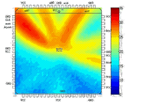
Material consistency plays a pivotal role—using high-grade substrates with tightly controlled dielectric properties ensures signal integrity, while precision stenciling techniques maintain uniform solder paste deposition. For complex multilayer boards, laser-drilled microvias and impedance-controlled routing are critical to minimizing signal loss in high-frequency applications.
Notably, the transition from prototype to full-scale PCBA production demands rigorous process calibration. Implementing statistical process control (SPC) charts for key parameters—such as reflow oven temperature profiles or pick-and-place machine accuracy—helps sustain tolerances within ±1% across batches. This systematic approach not only reduces rework rates but also aligns with the broader goal of balancing speed and quality in subsequent manufacturing stages.

Balancing Speed and Quality in PCB Assembly
Achieving equilibrium between rapid production timelines and consistent output standards remains a critical challenge in PCB assembly. Manufacturers must implement design-for-manufacturability (DFM) principles early in the prototyping phase to minimize rework while accelerating PCBA workflows. Automated optical inspection (AOI) systems and precision solder paste application techniques enable faster cycle times without compromising defect detection rates. However, prioritizing speed alone risks overlooking subtle flaws, such as microvoids in ball grid arrays or misaligned components, which escalate long-term reliability concerns.
To address this, lean manufacturing methodologies paired with real-time process monitoring create a framework where cycle time reductions align with stringent quality benchmarks. For instance, combining high-speed surface-mount technology (SMT) with inline X-ray inspection ensures rapid placement accuracy verification. Additionally, optimizing panelization layouts reduces material waste while maintaining electrical testing efficiency.
Strategic partnerships with suppliers for verified materials and pre-programmed component feeders further streamline PCB assembly stages. By balancing advanced automation with rigorous testing protocols, manufacturers can deliver PCBA outputs that meet both accelerated deadlines and performance expectations, proving that speed and quality are not mutually exclusive in modern electronics production.
PCB Assembly Quality Control Best Practices
Implementing rigorous quality control measures remains critical for achieving reliable PCB assembly outcomes. Modern PCBA workflows integrate automated optical inspection (AOI) systems to detect solder joint defects, component misalignment, and trace irregularities with micron-level accuracy. Statistical process control (SPC) methodologies further enhance consistency by analyzing production data to identify deviations in surface-mount technology (SMT) placement or reflow soldering parameters.
For high-density interconnect (HDI) boards, X-ray inspection becomes indispensable for verifying blind via integrity and ball grid array (BGA) connections. To balance efficiency and precision, manufacturers often adopt first-article inspection (FAI) protocols, validating initial production units against design specifications before full-scale runs.
Transitioning between inspection stages requires seamless coordination between automated test equipment (ATE) and manual verification teams. Prioritizing traceability through barcoding or RFID tagging ensures rapid defect root-cause analysis, particularly in mixed-technology assemblies combining through-hole components with advanced SMT parts. By embedding these practices into PCBA workflows, manufacturers reduce rework rates by 18–35% while maintaining ISO 9001 compliance thresholds.
Troubleshooting Common Prototype Fabrication Flaws
Identifying and resolving fabrication flaws early in PCB assembly processes is critical to preventing costly delays. Common issues such as misaligned solder pads, insufficient copper traces, or thermal stress fractures often stem from design inconsistencies or material mismatches. For instance, acid traps in complex layouts can lead to incomplete etching, while improper stencil thickness during PCBA stages may cause solder bridging.
To mitigate these risks, implement automated optical inspection (AOI) systems to detect anomalies in real time. Cross-referencing design files with physical prototypes using 3D X-ray imaging helps uncover hidden defects like voids in ball grid arrays (BGAs). When addressing thermal management flaws, verify that substrate materials align with operational temperature ranges and adjust reflow profiles accordingly.
Collaboration between design and manufacturing teams is essential. For example, revising pad geometries to accommodate smaller components or optimizing panelization layouts can reduce PCB assembly errors. Additionally, conducting impedance testing on high-speed circuits ensures signal integrity before full-scale production. By systematically diagnosing root causes and refining processes, manufacturers can enhance PCBA reliability while maintaining alignment with broader quality control frameworks.
Advanced PCB Manufacturing Process Innovations
Recent advancements in PCB assembly technologies are reshaping how manufacturers approach prototyping and production. Innovations such as additive manufacturing enable rapid iteration of PCBA designs by layering conductive materials with micron-level precision, reducing material waste by up to 30%. Automated optical inspection (AOI) systems, integrated with machine learning algorithms, now detect defects in real time during PCB assembly, improving yield rates while cutting inspection time by half. Additionally, the adoption of high-density interconnect (HDI) substrates allows for compact, multi-layered designs without compromising signal integrity—a critical advantage for IoT and aerospace applications.
To further accelerate workflows, manufacturers are leveraging cloud-based collaboration platforms that synchronize design files with PCBA fabrication lines, minimizing delays between prototyping and mass production. Advanced soldering techniques, including laser reflow and selective soldering, ensure consistent joint quality even for micro-BGA components. Sustainability is also driving innovation, with biodegradable substrates and lead-free solder alloys gaining traction. These breakthroughs not only enhance precision but also align with global regulatory standards, ensuring that PCB assembly processes remain both efficient and environmentally responsible.
Conclusion
Effective optimization of PCB assembly processes requires a holistic approach that balances technical precision with operational efficiency. By integrating design-for-manufacturability principles early in the PCBA workflow, teams can mitigate delays and reduce material waste. Advanced tools like automated optical inspection (AOI) and real-time analytics further enhance quality control, ensuring that PCB prototype iterations meet exacting standards without compromising production timelines.
Adopting modular strategies for PCB assembly—such as standardized component libraries and flexible manufacturing setups—enables rapid scaling while maintaining cost predictability. For PCBA projects, leveraging collaborative supplier networks and predictive maintenance protocols minimizes downtime and accelerates time-to-market. Additionally, aligning fabrication workflows with Industry 4.0 frameworks ensures seamless data exchange between prototyping and full-scale production phases.
Ultimately, the convergence of agile methodologies and precision engineering in PCB assembly creates a foundation for sustainable innovation. As manufacturers adopt smarter tools and refine process hierarchies, the gap between prototype validation and mass production continues to narrow, delivering both economic and technical advantages across the electronics lifecycle.
FAQs
How does proper PCB assembly planning reduce production delays?
Effective planning involves verifying design specifications before manufacturing begins. By conducting thorough DFM (Design for Manufacturing) checks, engineers can identify potential conflicts in component placement or routing, minimizing rework during PCBA stages.
What factors most impact costs in PCB prototype development?
Material selection, layer count, and turnaround time are primary cost drivers. Opting for standardized substrates and consolidating testing phases can lower expenses without compromising PCB assembly quality.
How can manufacturers balance speed and precision in PCBA?
Automated optical inspection (AOI) systems enable rapid defect detection, while modular assembly lines allow parallel processing. Implementing real-time monitoring ensures adherence to tolerances even under accelerated timelines.
What are common errors in prototype PCB assembly workflows?
Misaligned solder masks and insufficient thermal relief patterns frequently cause failures. Adopting simulation tools to model thermal and mechanical stresses during PCBA helps preempt these issues.
Why is component sourcing critical for reliable PCB assembly?
Supply chain inconsistencies lead to counterfeit parts or delivery delays. Partnering with certified suppliers and maintaining buffer inventories for critical components stabilizes PCBA production flows.
Ready to Streamline Your PCB Assembly Process?
For tailored solutions that enhance prototyping efficiency and PCBA reliability, please click here to explore advanced manufacturing strategies.