Optimizing Printed Wiring Assembly for Enhanced Performance

Key Takeaways
Optimizing printed wiring assembly (PWA) is crucial for enhancing the performance of electronic devices, particularly through advancements in PCB assembly (PCBA) methods. A primary takeaway is the significant impact that design efficiency has on the overall functionality of a PWA. By employing techniques that streamline circuit layouts and optimize component placement, manufacturers can not only reduce costs but also enhance signal integrity and reduce electromagnetic interference.
Furthermore, material selection plays a pivotal role; utilizing high-quality substrates and solder materials can lead to improved reliability and longevity of the assembly. As part of the optimization strategy, testing and quality assurance are indispensable. Regularly inspecting assembled boards for defects ensures that potential issues are identified early, thereby reducing failure rates in final products.
A helpful tip to remember is: > “Prioritize robust design principles to minimize errors in PCB assembly during the early stages of development.” This aligns with future trends indicating a growing focus on integrating automated quality checks within manufacturing processes.
In summary, through precise design techniques, careful material selection, and rigorous testing protocols, organizations can significantly enhance their PCBA’s performance while achieving superior functionality. A dedicated approach to these aspects not only fosters reliability but also positions companies to more effectively meet market demands with innovative electronic solutions.
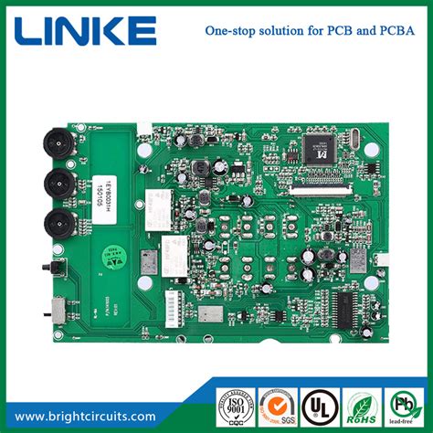
Introduction to Printed Wiring Assembly and Its Importance
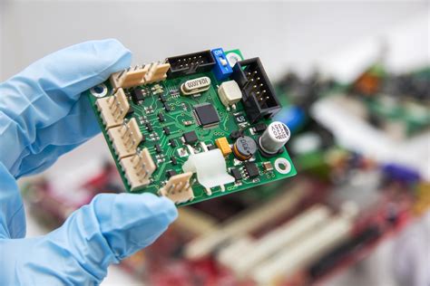
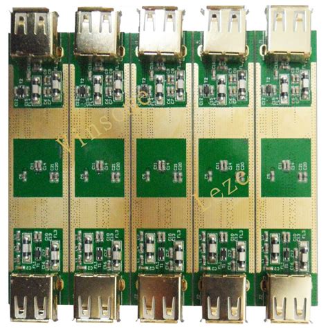
Printed Wiring Assembly (PWA) is a critical process in the field of electronics, serving as the backbone for modern electronic devices. The significance of PWA lies in its ability to integrate various electronic components onto a single printed circuit board (PCB), known as PCB assembly or PCBA. This integration not only streamlines the manufacturing process but also enhances functional efficiency and overall device reliability. As technology advances, optimizing the pcb assembly process becomes increasingly vital in meeting the growing demands for compactness, performance, and cost-effectiveness in electronic applications. Moreover, understanding the importance of effective PWA design leads to improved thermal management, reduced electromagnetic interference (EMI), and ultimately a longer lifespan for devices. Thus, mastering the intricacies of printed wiring assembly is essential for engineers and manufacturers striving to deliver innovative solutions while maintaining high standards of quality and durability in today’s competitive market.
Key Factors Influencing Printed Wiring Assembly Performance
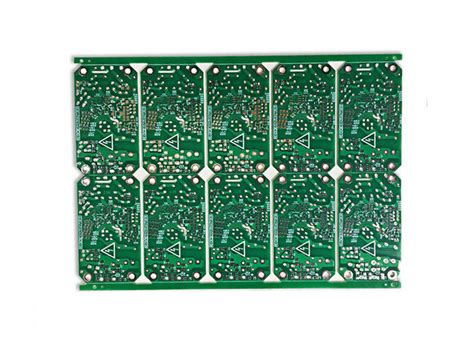
The performance of printed wiring assemblies (PCBA) is influenced by several critical factors that play a fundamental role in the efficacy and reliability of electronic devices. One of the primary aspects is design efficiency, which involves creating layouts that optimize space and enhance signal integrity while minimizing the potential for interference. Effective design reduces complexity, which is essential for scalability and eases the assembly process. Additionally, material selection significantly impacts performance. High-quality materials improve not only the durability of pcb assembly but also ensure better conductivity and thermal management, which are vital for maintaining device functionality in various operating conditions. Furthermore, advanced manufacturing processes contribute to the precision and accuracy required in modern assemblies. Techniques such as surface mount technology (SMT) are particularly noteworthy, as they allow for reduced component size and increased component density on boards. This juxtaposition of design, materials, and manufacturing methods underscores how a strategic approach to each element can significantly elevate the overall performance of printed wiring assemblies. It is crucial for manufacturers to evaluate these factors continually to innovate and stay competitive in an ever-evolving market landscape.
Design Efficiency Techniques for Printed Wiring Assembly
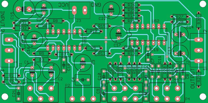
Achieving design efficiency in printed wiring assembly (PWA) is essential for enhancing the overall performance of pcb assembly operations. One of the primary techniques involves optimizing the layout of components to minimize space and reduce signal paths. By employing advanced design software, engineers can create compact and efficient layouts, which help to lower production costs and improve reliability. Additionally, utilizing design rule check (DRC) methods ensures that the assembly will comply with industry standards, preventing common issues such as short circuits or incorrect placements that can deteriorate performance.
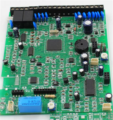
Another critical aspect is selecting the appropriate substrate materials and components, which directly influence the functionality of the final product. Using high-quality materials in your pcba not only ensures durability but also affects signal integrity and heat dissipation characteristics. Therefore, investing time in proper material selection can yield significant long-term benefits.
Moreover, integrating modular design approaches allows for flexibility in production—facilitating easier updates or repairs without necessitating complete redesigns. This adaptability becomes increasingly vital in today’s fast-paced technology landscape, allowing manufacturers to respond swiftly to changing demands.
To further improve efficiency, it’s essential to streamline communication between engineering and manufacturing teams to ensure that design specifications are accurately translated into production processes. By fostering a collaborative environment that emphasizes feedback during early development stages, organizations can identify potential challenges early on and implement solutions proactively.
Adopting these design efficiency techniques not only boosts productivity and effectiveness but also equips organizations with a competitive advantage in optimizing their printed wiring assemblies, ultimately leading to enhanced performance across electronic devices.
Testing and Quality Assurance in Printed Wiring Assembly
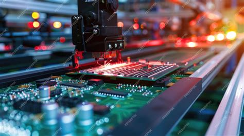
The success of printed wiring assembly (PWA), often referred to as pcb assembly or pcba, heavily relies on rigorous testing and quality assurance measures. These processes are fundamental to ensuring that the assembled circuits function reliably under various conditions. Critical components of an effective testing strategy include methods such as Automated Optical Inspection (AOI), X-ray inspection, and functional testing, which are employed to detect potential faults in the pcba before the final product reaches the consumer. Performing these tests not only helps in identifying electrical and mechanical issues but also enhances the overall efficiency of the manufacturing process by minimizing rework and ensuring adherence to industry standards. Moreover, establishing a robust quality assurance framework facilitates consistent monitoring throughout production, enabling manufacturers to trace defects back to specific stages of the assembly process. This traceability not only aids in rectifying existing issues but also informs future design iterations by providing valuable insights into component performance and PCB layout effectiveness. Through these meticulous testing and quality assurance practices, manufacturers can significantly enhance the performance and longevity of their printed wiring assemblies while instilling confidence in end-users regarding product reliability.
Case Studies: Successful Optimization of Printed Wiring Assemblies
In the realm of pcb assembly, several exemplary case studies illustrate the significant impact of optimization strategies. One notable case involved a leading electronics manufacturer that aimed to enhance the performance and reliability of their pcba used in consumer electronics. By prioritizing design efficiency, the team implemented advanced computer-aided design tools, which allowed for intricate layouts that minimized signal interference and enhanced thermal management. Additionally, through meticulous material selection, the manufacturer opted for high-quality substrate materials that boasted superior dielectric properties, further boosting signal integrity.
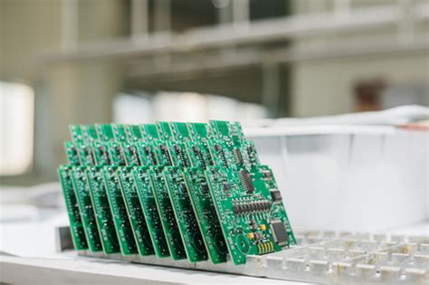
Moreover, a shift in their manufacturing processes—incorporating automated assembly technologies—reduced defects and improved production speed. This transition not only cut down on costs but also aligned with sustainability goals by optimizing material usage and reducing waste. Regular testing protocols ensured that each printed wiring assembly met rigorous performance standards. Overall, these case studies highlight that through focused strategies in design, materials, and production techniques, companies can achieve remarkable enhancements in their pcb assembly operations while maintaining unparalleled functionality and reliability in electronic devices.
Future Trends in Printed Wiring Assembly Optimization
As technology continues to evolve, the demand for more efficient and reliable pcb assembly processes is becoming increasingly critical. One prominent trend in the optimization of pcba is the integration of advanced materials that not only enhance performance but also reduce costs. For instance, the use of flexible substrates can lead to lighter and thinner electronic devices, an essential factor in today’s portable electronics market. Additionally, automation in manufacturing processes is expected to streamline production, minimizing human error and maximizing consistency in printed wiring assembly. Implementing intelligent design software that utilizes machine learning algorithms is another emerging trend; these tools can analyze performance data and suggest modifications that help achieve optimal designs. Furthermore, the move toward environmentally friendly manufacturing practices will likely influence material selection strategies, with an increased focus on sustainability and recyclability in component choices. Overall, the future of printed wiring assembly optimization lies in harmonizing innovative technologies with efficient practices to drive enhanced functionality and reliability within electronic devices.
Conclusion
In summary, optimizing printed wiring assembly (PWA) is crucial for enhancing the performance and reliability of electronic devices. By focusing on key factors such as design efficiency, material selection, and streamlined manufacturing processes, organizations can achieve superior outcomes in their pcb assembly efforts. The careful integration of advanced design techniques can lead to a more compact layout, reducing signal loss and electromagnetic interference. Moreover, selecting the right materials ensures that the pcba not only meets but exceeds standard performance metrics, promoting longevity and resilience under varying operational conditions. Continuous advancements in technology also allow for improved testing methods and quality assurance protocols that further enhance the reliability of printed wiring assemblies. Ultimately, it is these strategic optimizations that pave the way for innovative products capable of meeting the evolving demands of consumers and industries alike.
FAQs
What is printed wiring assembly (PWA)?
Printed wiring assembly, commonly referred to as pcb assembly, is a process where electronic components are mounted onto a printed circuit board (PCB) to form a complete assembly ready for use in electronic devices.
Why is design efficiency important in PCB assembly?
Design efficiency enhances the overall functionality of the pcba by ensuring optimal layout and component placement, which significantly impacts manufacturing time and production costs.
What factors should be considered in material selection for printed wiring assemblies?
Selecting materials with suitable electrical, thermal, and mechanical properties is crucial. Factors such as conductivity, dielectric strength, and thermal stability play a vital role in ensuring that the pcb assembly meets performance expectations.
How can manufacturing processes be improved for printed wiring assemblies?
Continuous improvement in manufacturing techniques—like automated soldering, efficient component placement, and streamlined workflow—can significantly enhance the quality and reliability of pcba, ultimately leading to better performance.
What role does testing play in ensuring quality assurance for PCB assemblies?
Testing methods such as functional testing, in-circuit testing, and thermal cycle tests are essential in identifying potential faults and ensuring that each pcb assembly adheres to strict quality standards.