Optimizing Signal Transmission: Multilayer PCB Design Essentials
Key Takeaways
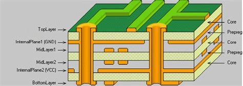
When designing multilayer printed circuit boards, understanding foundational principles ensures reliable signal transmission and cost efficiency. Start by prioritizing layer stackup configurations—a well-planned arrangement of power, ground, and signal layers minimizes electromagnetic interference (EMI) and optimizes thermal management. For example, symmetrical stackups with adjacent ground planes shield high-speed signals, reducing crosstalk by up to 40% in dense layouts.
Material selection directly impacts performance and pcb manufacturing cost. High-frequency applications demand low-loss substrates like Rogers 4350B, while cost-sensitive projects may opt for FR-4. Partnering with experienced pcb manufacturing companies ensures material choices align with your design’s electrical and budgetary constraints.
| Layer Configuration | Key Benefit | Typical Use Case |
|---|---|---|
| 4-layer (S-G-P-S) | Balanced EMI shielding | Consumer electronics |
| 6-layer (S-G-S-P-G-S) | Enhanced signal integrity | Networking equipment |
| 8-layer+ | Ultra-high-speed isolation | Aerospace/medical systems |
Impedance control is non-negotiable for high-speed designs. Use field solvers to calculate trace widths and dielectric spacing, aiming for tolerances below ±10%. During pcb manufacturing, specify controlled impedance testing to verify compliance—a step often overlooked in low-cost pcb manufacturing business models, leading to signal degradation.
To minimize crosstalk, route critical signals orthogonally across adjacent layers and maintain a 3W rule (trace spacing ≥ 3x trace width). Post-layout simulations with tools like HyperLynx identify hotspots before prototyping, saving time and revisions.
Finally, balance performance with pcb manufacturing cost by optimizing layer counts. While more layers improve signal integrity, they escalate production expenses. For prototypes, consider partnering with agile manufacturers like Andwin PCB & Assembly to validate designs before scaling. Testing signal quality with TDR (Time-Domain Reflectometry) and eye diagrams ensures your multilayer PCB meets specifications without over-engineering.
By integrating these strategies, you’ll achieve robust designs that satisfy both technical requirements and economic realities in modern pcb manufacturing.
Multilayer PCB Stackup Design Essentials
When designing multilayer PCBs, your stackup configuration directly impacts signal integrity, thermal management, and pcb manufacturing cost. Start by defining the number of layers based on your circuit’s complexity—high-speed designs often require 6-12 layers to isolate sensitive signals and power planes. A symmetrical stackup minimizes warping during pcb manufacturing, ensuring reliability across temperature fluctuations. For example, placing high-speed signal layers adjacent to ground planes reduces electromagnetic interference (EMI), while alternating core and prepreg materials balances mechanical stability.
Collaborating with experienced pcb manufacturing companies early in the design phase helps optimize material selection. FR-4 remains cost-effective for standard applications, but high-frequency systems may demand low-loss laminates like Rogers 4350B. These choices influence pcb manufacturing business workflows, as specialized materials often require adjusted lamination cycles. Always verify dielectric constants (Dk) and loss tangents (Df) with your manufacturer to align simulation models with real-world performance.
Impedance control is non-negotiable for consistent signal transmission. Use field solvers to calculate trace widths and spacing, factoring in the copper weight and dielectric thickness of each layer. Tight tolerances (±5-10%) are achievable through precise pcb manufacturing processes like laser direct imaging (LDI). Remember, impedance mismatches not only degrade signals but also increase rework costs—a critical consideration for balancing pcb manufacturing cost with quality.
Finally, incorporate test coupons into your panel layout to validate layer alignment and impedance during fabrication. This proactive step reduces post-production surprises and strengthens partnerships with pcb manufacturing companies by streamlining quality checks. By prioritizing stackup symmetry, material compatibility, and impedance accuracy, you create boards that perform reliably while maintaining scalable production economics.
High-Speed Signal Integrity Strategies
Maintaining signal integrity in high-speed multilayer PCBs requires balancing design precision with PCB manufacturing realities. Start by defining a controlled impedance environment through careful trace geometry planning. Use differential pairs for critical signals, ensuring symmetrical routing to minimize skew and electromagnetic interference (EMI). PCB manufacturing companies often recommend ground planes adjacent to signal layers to reduce noise coupling—a practice that also enhances thermal management.
"For high-frequency designs, prioritize materials with low dielectric loss (Df) and consistent dielectric constants (Dk) across operating temperatures. This reduces phase distortion and ensures predictable signal behavior."
When implementing via structures, optimize their placement to avoid impedance discontinuities. Back-drilling or using blind/buried vias from trusted PCB manufacturing business partners can mitigate stub effects in signals above 5 GHz. Simulations play a pivotal role here—tools like 3D electromagnetic field solvers identify resonance issues early, preventing costly redesigns.
Impedance mismatches often stem from inconsistent PCB manufacturing cost decisions, such as using suboptimal copper roughness. Specify smooth rolled copper foils for inner layers to minimize skin effect losses in signals exceeding 10 Gbps. Pair this with surface finishes like immersion silver or ENIG to maintain solderability without degrading high-frequency performance.
To address crosstalk, adhere to the 3W rule (trace spacing ≥3× trace width) and route adjacent layers orthogonally. Advanced PCB manufacturing techniques, such as hybrid stackups combining FR-4 with high-speed laminates (e.g., Rogers 4350B), allow cost-effective performance tuning. Always validate designs with time-domain reflectometry (TDR) testing to confirm impedance tolerances stay within ±5%.
"Collaborate with fabricators during the stackup design phase—their expertise in material availability and process limitations directly impacts both signal quality and project timelines."
By integrating these strategies, you ensure that high-speed signals traverse multilayer boards with minimal distortion, aligning technical requirements with practical PCB manufacturing constraints.
Material Selection for Optimal Performance
When selecting materials for multilayer PCB design, balancing electrical performance, thermal stability, and pcb manufacturing cost requires careful analysis. The dielectric constant (Dk) and dissipation factor (Df) of substrate materials directly influence signal integrity, particularly in high-speed applications. Low-loss laminates like Rogers 4350B or Isola FR408HR minimize signal attenuation, but their higher costs may necessitate trade-offs for budget-sensitive projects.
For pcb manufacturing companies, thermal management is another critical factor. Materials with high glass transition temperatures (Tg > 170°C) and low coefficients of thermal expansion (CTE) ensure reliability during repeated thermal cycling. This becomes particularly important in applications like automotive electronics or aerospace systems, where temperature fluctuations can degrade interlayer connections. High-Tg FR-4 remains a cost-effective choice for many designs, though advanced polyimide-based substrates may be required for extreme environments.
Impedance control demands precise dielectric thickness consistency, which ties directly to pcb manufacturing business capabilities. Partnering with fabricators that offer tight tolerance controls (≤±10%) ensures predictable performance across production batches. Additionally, copper foil roughness affects high-frequency losses—smoother rolled copper surfaces reduce skin effect losses but may increase material costs.
In high-density designs, material selection also impacts manufacturability. For example, laser-drillable prepregs enable finer microvia structures, but compatibility with your fabricator’s equipment must be verified early. Balancing these technical requirements with pcb manufacturing realities—such as material lead times and scalability—requires collaboration between design engineers and fabrication partners to optimize both performance and production efficiency.
Impedance Control in Multilayer Circuits
Achieving precise impedance control in multilayer PCBs requires balancing design precision with material science. When working with high-speed signals, even minor deviations in trace geometry or dielectric properties can degrade signal integrity, leading to reflections or data errors. You’ll need to define target impedance values early in the design phase, factoring in the operating frequency, signal rise times, and the interaction between adjacent layers.
Critical to this process is selecting materials with consistent dielectric constants (Dk) and loss tangents. For example, FR-4 may suffice for lower-frequency applications, but high-speed designs often demand specialized laminates like Rogers or Isola substrates. Layer stackup configuration directly impacts impedance—thinner dielectrics reduce cross-sectional area, increasing capacitance, while wider traces lower inductive reactance. Modern PCB manufacturing companies use field solvers to simulate impedance across different layer combinations, ensuring compliance with ±10% tolerance standards common in industries like telecommunications.
Collaborate closely with your PCB manufacturing partner to validate controlled impedance requirements. They’ll typically adjust trace widths, copper weights, or dielectric thicknesses during prototyping to compensate for production variances. Keep in mind that tighter impedance tolerances escalate PCB manufacturing cost due to additional testing steps, such as time-domain reflectometry (TDR) or coupon-based verification. For cost-sensitive projects, prioritize impedance-critical layers (e.g., outer signal layers) while relaxing tolerances on less sensitive internal planes.
In high-density designs, avoid impedance discontinuities at vias or connectors by implementing back-drilling or via-in-pad techniques. Symmetrical stackups also help maintain consistent impedance paths across differential pairs. When optimizing for PCB manufacturing business scalability, document impedance profiles in fabrication notes and request impedance test reports to ensure repeatability across production batches.
Remember: effective impedance control isn’t just theoretical—it demands iterative testing. Partner with manufacturers offering real-time impedance monitoring during mass production to catch deviations before they escalate into field failures.
Crosstalk Reduction Techniques Explained
Effective crosstalk management begins with understanding how electromagnetic coupling between adjacent traces degrades signal quality. To minimize interference, prioritize differential pair routing for high-speed signals, ensuring matched trace lengths and consistent spacing. Implementing ground planes between active signal layers acts as a shield, absorbing stray fields that cause unwanted coupling. When working with pcb manufacturing companies, specify controlled impedance requirements early in the design phase to align their fabrication processes with your noise reduction goals.
For dense layouts, increase trace-to-trace separation to at least three times the dielectric thickness—a rule often overlooked when optimizing pcb manufacturing cost. Guard traces grounded through vias at regular intervals create isolation barriers, particularly useful for clock lines or other aggressor signals. Advanced pcb manufacturing techniques like embedded capacitance layers can further suppress power plane noise, a common contributor to crosstalk in multilayer designs.
Signal layer arrangement significantly impacts cross-talk performance. Position adjacent signal layers orthogonally (horizontal vs. vertical routing) to reduce overlap, and sandwich high-speed layers between solid reference planes. When evaluating pcb manufacturing business proposals, verify their capability to maintain precise dielectric thickness—variations as small as 10% can alter coupling coefficients.
Simulation tools prove invaluable for pre-fabrication analysis. Perform 3D electromagnetic field modeling to identify potential coupling hotspots, adjusting trace spacing or adding termination resistors as needed. For cost-sensitive projects, balance pcb manufacturing cost with performance by reserving premium materials like low-loss laminates only for critical signal layers.
Remember that via placement influences crosstalk through parasitic inductance. Cluster vias away from sensitive analog sections and implement back-drilling for high-frequency designs to remove unused via stubs. These measures, when coordinated with your pcb manufacturing partner’s capabilities, create a robust defense against signal integrity issues without unnecessary complexity.
Layer Configuration Best Practices
When designing multilayer printed circuit boards, layer stackup configuration directly impacts signal integrity, thermal management, and PCB manufacturing cost. Begin by separating high-speed signal layers with ground planes to minimize electromagnetic interference—a critical step for maintaining clean signal paths in dense layouts. For boards with 6-12 layers, adopt a symmetrical stackup to prevent warping during fabrication, which PCB manufacturing companies often emphasize to ensure yield rates.
Prioritize placing sensitive analog traces on inner layers sandwiched between power and ground planes, shielding them from digital noise. Use low-loss dielectric materials (e.g., FR-4 High-Tg or Rogers substrates) for high-frequency applications, but verify their compatibility with your PCB manufacturing business partner’s capabilities to avoid cost overruns. A 4-layer board, for instance, might follow a Signal-Ground-Power-Signal arrangement, while an 8-layer design could integrate dedicated routing layers for differential pairs and controlled impedance signals.
Another critical consideration is via placement. Minimize stub lengths by using blind or buried vias for high-speed transitions, though this increases PCB manufacturing cost due to added process complexity. For cost-sensitive projects, work with your fabricator to optimize through-hole via patterns without compromising signal quality. Always allocate separate layers for power distribution networks (PDNs) to reduce voltage drops and stabilize supply rails—a practice that enhances reliability in mission-critical systems.
When collaborating with PCB manufacturing partners, provide detailed impedance profiles and material specifications early in the design phase. This alignment ensures layer thicknesses and copper weights match your signal requirements while keeping fabrication feasible. Remember: a well-planned layer configuration not only boosts performance but also streamlines production timelines, directly affecting your project’s scalability and profitability.
Testing Multilayer PCB Signal Quality
Validating signal integrity in multilayer PCB manufacturing demands a systematic approach to identify and resolve transmission anomalies. High-speed signals face challenges like timing skew, reflection, and attenuation, which intensify as layer counts increase. Start by employing time-domain reflectometry (TDR) to pinpoint impedance mismatches in traces, ensuring alignment with your design’s target values (e.g., 50Ω or 100Ω differential). For radio-frequency applications, vector network analyzers (VNAs) provide critical insights into insertion loss and return loss across frequency ranges up to 40 GHz or higher.
When partnering with PCB manufacturing companies, verify their capability to perform automated flying probe tests or boundary-scan diagnostics. These methods detect opens, shorts, and cross-talk between adjacent layers—common culprits in signal degradation. Advanced facilities may also offer eye diagram analysis to visualize jitter and noise margins, particularly for interfaces like PCIe or DDR4.
A key cost driver in PCB manufacturing cost stems from post-production rework due to undetected signal flaws. To mitigate this, integrate pre-layout simulations using tools like HyperLynx or ANSYS HFSS. These predict electromagnetic interference (EMI) hotspots and validate termination strategies before fabrication begins. For example, simulating via stub effects in 12-layer boards can reduce resonance-induced distortions by up to 30%.
Material choices directly influence test outcomes. Low-loss laminates such as Rogers 4350B or Isola FR408HR minimize dielectric losses at higher frequencies but require tighter impedance control during lamination. Collaborate with your PCB manufacturing business partner to review their process controls for layer alignment and copper roughness, as these factors directly impact signal attenuation.
Finally, correlate physical measurements with design specifications using statistical analysis. Metrics like bit error rate (BER) and signal-to-noise ratio (SNR) quantify performance gaps, enabling iterative refinements. By combining rigorous testing protocols with proactive design adjustments, you balance PCB manufacturing cost constraints with uncompromised signal fidelity in complex multilayer systems.
Cost-Effective Manufacturing Tips
To balance performance and affordability in pcb manufacturing, start by collaborating early with experienced pcb manufacturing companies. Their engineers can identify design optimizations that reduce pcb manufacturing cost without compromising signal integrity—like suggesting alternative substrate materials or adjusting trace geometries to maintain impedance while using standard fabrication processes.
Another critical factor is layer stack-up planning. While minimizing layers lowers production expenses, ensure your configuration still meets shielding and high-speed routing needs. For example, combining power and ground planes in adjacent layers can reduce total layer count while preserving noise suppression.
When implementing design for manufacturing (DFM) principles, standardize hole sizes and avoid extremely tight tolerances unless absolutely necessary. This prevents specialized tooling requirements that escalate costs in pcb manufacturing business operations. Panelization also plays a key role: working with your manufacturer to arrange multiple boards per panel maximizes material usage and reduces waste.
For impedance-controlled designs, clearly specify tolerance ranges during design reviews. Overly strict requirements often lead to higher rejection rates and rework costs. Many pcb manufacturing companies offer cost-effective testing strategies, such as sampling rather than full-batch inspection, to verify signal quality without inflating budgets.
Lastly, consider long-term partnerships with manufacturers. Volume commitments or multi-project agreements often unlock better pricing structures, making your pcb manufacturing cost more predictable over time. Regularly review material inventories and process efficiencies with your supplier to identify new savings opportunities as technologies evolve.
Conclusion
Designing multilayer printed circuit boards demands a balance between technical precision and practical pcb manufacturing cost considerations. When executed properly, optimized layer stackups and impedance-matching strategies not only enhance signal integrity but also streamline production workflows for pcb manufacturing companies. The choice of materials—whether high-frequency laminates or low-loss dielectrics—directly impacts both performance and long-term reliability, making collaboration with experienced pcb manufacturing business partners critical for cost-effective outcomes.
Keep in mind that reducing crosstalk and maintaining consistent impedance requires rigorous simulation and prototyping, which may influence pcb manufacturing timelines. However, investing in these steps minimizes post-production revisions, ultimately lowering total project expenses. For high-speed designs, prioritize symmetrical layer configurations and ground-plane shielding to mitigate electromagnetic interference—a common pain point in dense multilayer layouts.
Finally, always validate your design through signal integrity testing before finalizing with pcb manufacturing providers. This ensures compliance with performance benchmarks while avoiding costly redesigns. By aligning your engineering decisions with manufacturing realities, you can achieve robust, high-performance boards without exceeding budget constraints—a cornerstone of sustainable pcb manufacturing business practices in today’s competitive electronics landscape.
FAQs
How does layer count affect pcb manufacturing cost?
The number of layers directly impacts pcb manufacturing cost due to increased material usage, production time, and complexity. While 8-12 layers are common for high-speed designs, exceeding 16 layers may require specialized equipment, raising expenses. Work with pcb manufacturing companies to balance performance needs with budget constraints.
What criteria should guide material selection for multilayer PCBs?
Prioritize dielectric constant (Dk) and loss tangent (Df) to minimize signal loss. Materials like FR-4 are cost-effective for standard applications, but high-frequency designs often require advanced substrates like Rogers. Discuss thermal and mechanical requirements with your pcb manufacturing business partner early in the design phase.
How can impedance mismatches be avoided in dense layouts?
Use controlled impedance routing and ensure consistent trace geometry. Most pcb manufacturing companies provide impedance calculators or simulation tools to validate stackup configurations. Always specify impedance tolerances (±10% typical) during fabrication to maintain signal integrity.
Does reducing pcb manufacturing cost compromise reliability?
Not necessarily. Optimize layer stackup to eliminate redundant planes, select cost-effective materials for non-critical layers, and standardize via sizes. Reputable pcb manufacturing partners can suggest design-for-manufacturing (DFM) adjustments that cut costs without sacrificing performance.
What testing methods ensure signal quality in multilayer PCBs?
Time-domain reflectometry (TDR) verifies impedance consistency, while network analyzers validate high-frequency performance. Many pcb manufacturing businesses offer automated optical inspection (AOI) and boundary scan testing to detect physical defects impacting signal paths.
Need Expert Guidance for Your Project?
For tailored solutions in pcb manufacturing that align with your design and budgetary needs, please click here to consult with industry specialists.


