PADs Tutorial: Software Function Introduction
Pads is a software for making PCBs. Most people in the electronics industry should have come into contact with pads software. The ease of use of pads software is also one of the reasons why pads is popular. In order to enhance everyone’s understanding of pads software, this article will introduce the many functions included in pads software. If you are interested in pads software, you may wish to continue reading with the editor.
Shell: Basic software operating environment (graphical interface), supporting complex PCB designs of any size;
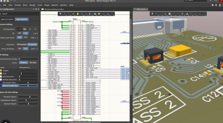
PCB Editor: Basic PCB design module, including manual layout and routing, design rule checking (DRC), manual copper plating, engineering modification command (ECO), pad and via library editing, Gerber data output and other functions;
Library Module: Component library management module, supporting operations such as adding and deleting library files, adding, deleting and editing component package symbols in the library, and supporting the function of creating library files from PCB files;
DXF Link: Bidirectional conversion interface for DXF format files, which can import PCB board frames drawn in mechanical software such as AutoCAD, and can also export the current PCB design as DXF format data;
CCT Link: Interface for data conversion with Cadence Specctra PCB router;
On-Line Design Rule Checking: Real-time design rule checking module, which can monitor the designer’s operations in real time and promptly prevent operations that may violate design rules such as line length, line width, spacing, etc. Designers can start/stop On-Line DRC as needed;
Auto Dimensioning: Automatic dimensioning module, providing automatic dimensioning function in accordance with international standards. The annotation content can be the length, radius, angle and other parameters of design content such as components or PCB board frame;
Split Planes: Power layer network definition and segmentation module, providing functions such as creating copper borders, copper border definition, power segmentation according to PCB board frame, and supporting power network nesting;
CAM Plus: Automatic assembly data output module, supporting automatic patch insertion machines in formats such as Dyanpert, Universal, and Phillips;
Cluster Placement: Automatic layout module, which can define all components on the PCB as different modules according to circuit relationships, realize collective movement, rotation and other layout operations of the entire module, and support automatic layout;
Assembly Variants: Variable management module of production material list, supporting the derivation of production material lists of different specifications from one PCB design to meet the needs of material preparation and processing of products of different grades and models, and can set options such as installation or replacement of different components on the PCB;
Physical Design Reuse (PDR): Design reuse module, supports the preservation of classic circuit PCB modules and repeated calls in different designs. When executing design reuse, the software will automatically check the current schematic design and automatically update the component position number in the reused module to ensure the consistency of the schematic and PCB data before and after reuse;
DFF Audit: Manufacturability inspection module, checks the design details on the PCB that are prone to cause manufacturing obstacles such as solder bridges, acid trips, copper/solder mask slivers, and annular rings;
Enhanced Analog Tool Kit with Array Placement: Analog PCB design tool kit, including jumpers (variable length/angle), teardrops (straight/concave teardrops, variable size), special-shaped pads and other functions commonly used in single/double-sided PCB design, as well as polar coordinate layout, synchronous rotation of multiple packages, and automatic routing at any angle and other functions commonly used in circular PCB design;
PADS Router (FIRE) :Fast interactive manual router, which can use interactive routing functions for complex PCBs of any size, supporting bus routing, automatic connection, routing path planning, routing shape optimization, dynamic routing/via pushing, automatic centering, automatic adjustment of line width and other functions;
PADS Router HSD (FIRE HSD): Fast interactive manual high-speed routing module, supporting interactive routing of differential pair signals, interactive serpentine lines, fixed-length/limited-length signals, and delay matching groups,
Enhanced DFT Audit: Advanced PCB testability inspection module, which can automatically add test points to all networks on the PCB, optimize test point routing, and mark networks that cannot be tested. Supports PCB ICT (In Circuit Testing) automatic test equipment, which can output test point data that meets IPC standards;
Advanced RuleSet: Advanced design rule definition module, including hierarchical design rule definition, high-speed design rule definition, and signal impedance and delay calculation. This module can be used to construct multi-level constraints for PCB design, such as different layout and routing rules for different types of networks, pin pairs (PinPair) and packages; it can define design rules such as differential pairs, limiting maximum crosstalk impedance, fixed-length/limited-length signals and delay matching groups, and automatically adjusting line widths of the same network at different layers to achieve impedance continuity; it can also calculate the impedance and delay of PCB routing;
IDF (ProE) Link: a two-way data conversion interface of the three-dimensional mechanical design software ProE, which can export PCB design files to ProE to view the three-dimensional display effect of PCB design, and can also import the plane size, height and other parameters of components modified in ProE;
PADS Autorouter (BlazeRouter): an intelligent automatic router that can automatically route, optimize routing, fan out components and optimize vias for any multi-layer complex PCB.