Panasonic Megtron 6: Advancing High-Speed Circuit Performance
Key Takeaways
When selecting materials for high-frequency applications, PCB manufacturing demands precision to balance performance and PCB manufacturing cost. Panasonic Megtron 6 stands out as a next-generation laminate engineered for 5G infrastructure and advanced networking equipment, offering ultra-low signal loss and thermal stability up to 410°C. For PCB manufacturing companies, this translates to enhanced reliability in high-density interconnect (HDI) designs, where minimizing dielectric constant (Dk) and dissipation factor (Df) is critical for maintaining signal integrity.
Here’s how Megtron 6 compares to conventional materials:
| Attribute | Megtron 6 | Traditional FR-4 |
|---|---|---|
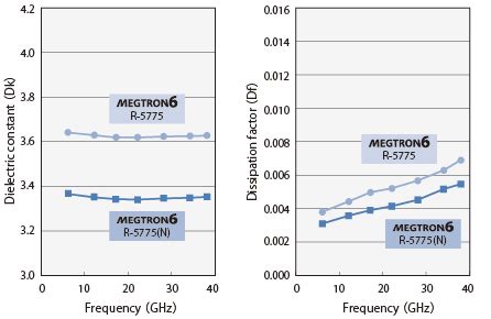
| Dk/Df (10 GHz) | 3.7/0.0015 | 4.5/0.020 |
| Thermal Resistance | 410°C | 130°C |
| Signal Loss | <0.4 dB/inch @ 10 GHz | >0.8 dB/inch @ 10 GHz |
| Compliance | IPC-4101/126 | Limited to lower tiers |
For PCB manufacturing businesses, adopting Megtron 6 reduces retooling costs by enabling compatibility with existing processes while meeting IPC standards. Its low Dk/Df properties allow tighter trace spacing without compromising performance—essential for millimeter-wave applications in 5G base stations. You’ll also benefit from reduced insertion loss, which minimizes the need for signal boosters, lowering overall PCB manufacturing cost in complex RF designs.
When optimizing network equipment performance, prioritize materials that withstand thermal cycling and high-power workloads. Megtron 6’s glass transition temperature (Tg) of 180°C ensures stability in environments where traditional laminates degrade, making it a strategic choice for mission-critical infrastructure. Whether you’re scaling PCB manufacturing for data centers or IoT devices, this laminate bridges the gap between high-speed demands and long-term reliability.
Ultra-Low Loss PCBs for 5G Networks
When designing PCB manufacturing solutions for 5G infrastructure, signal loss becomes a critical bottleneck. Panasonic Megtron 6 addresses this challenge with its ultra-low dissipation factor (Df ≤ 0.0015 at 10 GHz), enabling high-frequency signals to travel farther with minimal degradation. This is especially vital for millimeter-wave applications in 5G base stations and antennas, where even minor losses can disrupt network reliability.
For PCB manufacturing companies, balancing performance and PCB manufacturing cost requires materials that reduce post-processing while meeting stringent electrical specs. Megtron 6’s low dielectric constant (Dk ~3.2) simplifies impedance control, allowing designers to use thinner layers without sacrificing signal integrity. This directly impacts production efficiency, as fewer iterations are needed to achieve target specifications. Additionally, its thermal resistance up to 410°C ensures stability during lead-free soldering—a key consideration for high-density interconnect (HDI) designs common in 5G hardware.
In the PCB manufacturing business, material selection directly influences long-term ROI. Traditional FR-4 laminates, while cost-effective, struggle with high-speed signal demands. Megtron 6’s ultra-low loss properties extend equipment lifespan by minimizing heat generation and signal distortion, reducing maintenance costs for network operators. Collaborating with specialized partners like Andwin PCB can further optimize designs, leveraging advanced materials to meet 5G’s strict latency and bandwidth requirements.
As 5G networks scale, the need for PCB manufacturing solutions that combine precision and durability becomes non-negotiable. Megtron 6 not only supports tighter trace spacing for HDI layouts but also complies with IPC-4103 standards, ensuring consistency across batches. This reliability is crucial for applications ranging from massive MIMO antennas to edge computing servers, where material performance defines operational success.
High-Speed Signal Integrity Solutions
When designing circuits for 5G infrastructure or advanced networking equipment, maintaining signal integrity becomes critical as frequencies push beyond 10 GHz. Panasonic Megtron 6 addresses this challenge with its ultra-low dielectric properties (Dk of 3.7 and Df of 0.0015 at 10 GHz), which minimize signal distortion and attenuation even in densely routed PCB manufacturing layouts. By using materials that reduce insertion loss by up to 30% compared to standard FR-4 laminates, you ensure cleaner signal transmission—a non-negotiable requirement for high-speed data processing.
Tip: Always verify the glass transition temperature (Tg) and thermal expansion rate of your PCB substrate. Megtron 6’s 410°C heat resistance prevents warping during reflow soldering, maintaining layer alignment in HDI designs where even micron-level shifts degrade performance.
For PCB manufacturing companies, this material’s consistency across temperature fluctuations translates to fewer production defects. Its low Dk/Df variability (±2%) allows precise impedance control, reducing the need for costly post-fabrication tuning. When optimizing PCB manufacturing cost, consider how Megtron 6’s durability lowers failure rates in field deployments—a key factor for telecom providers managing network uptime SLAs.
“Signal integrity isn’t just about speed; it’s about reliability under real-world operating stresses,” notes a senior engineer at a leading networking OEM.
The laminate’s smooth copper interface further reduces skin effect losses at high frequencies, making it ideal for millimeter-wave applications. For PCB manufacturing businesses serving automotive radar or AI server markets, this combination of electrical and thermal stability future-proofs designs against evolving performance demands. When partnering with fabricators, prioritize those with expertise in handling low-loss materials to avoid compromises in layer bonding or drilling precision.
Megtron 6 Thermal Resistance Capabilities
When operating high-frequency circuits in demanding environments, managing heat becomes as critical as maintaining signal integrity. PCB manufacturing companies face unique challenges in balancing thermal performance with material costs, especially for applications like 5G base stations or data center infrastructure. Panasonic’s Megtron 6 addresses this by offering a glass-reinforced hydrocarbon laminate capable of withstanding temperatures up to 410°C during assembly processes like soldering or reflow.
This thermal resilience directly impacts PCB manufacturing cost by reducing warpage risks and minimizing defects caused by thermal stress. For designs requiring multiple layers or fine-pitch components, the material’s low coefficient of thermal expansion (CTE) ensures dimensional stability, even under rapid temperature cycling. In high-density interconnect (HDI) designs, where trace widths shrink below 50μm, this stability prevents microcracks that could compromise long-term reliability.
For PCB manufacturing businesses focused on advanced networking equipment, Megtron 6’s thermal properties complement its electrical advantages. The material maintains a stable dielectric constant (Dk ≤ 3.7) and dissipation factor (Df ≤ 0.0015) across temperatures ranging from -40°C to 125°C, ensuring consistent impedance control. This is vital for millimeter-wave frequencies in 5G NR systems, where even minor variations in heat distribution can degrade signal quality.
Moreover, the laminate’s IPC-4101/126 certification simplifies compliance for mission-critical applications. By integrating Megtron 6 into your stackup, you eliminate the need for additional thermal management layers in many cases, streamlining production workflows. This becomes particularly critical when scaling PCB manufacturing for large-volume orders, as it reduces reliance on costly post-processing steps like conformal coating or heatsink attachment.
The combination of ultra-low loss characteristics and robust thermal endurance positions Megtron 6 as a strategic choice for engineers designing next-gen wireless infrastructure. Whether optimizing power amplifier efficiency or ensuring signal integrity in server backplanes, its performance under thermal load directly translates to fewer field failures and lower total cost of ownership.
Advanced HDI Design with Low Dk/Df
When developing high-density interconnect (HDI) designs for next-generation networking hardware, selecting materials with stable dielectric properties becomes non-negotiable. Panasonic Megtron 6 addresses this need with its ultra-low Dk (dielectric constant) and Df (dissipation factor), enabling precise impedance control even in multilayer stack-ups. With a Dk of 3.7 at 10 GHz and a Df as low as 0.0015, signal attenuation drops significantly compared to standard FR-4 laminates. This ensures cleaner signal transmission across tightly spaced traces—a critical advantage for 5G base stations and high-frequency switches.
For PCB manufacturing companies, the material’s consistency directly impacts yield rates. Megtron 6’s low variance in dielectric values (±2% for Dk) minimizes redesign risks during prototyping, reducing PCB manufacturing cost overruns caused by impedance mismatches. Its compatibility with laser drilling and sequential lamination processes further supports fine-pitch microvias, a staple in HDI layouts. When paired with advanced plating techniques, the laminate maintains stable performance under thermal stress, avoiding delamination issues that plague traditional materials.
The business case for adopting Megtron 6 strengthens when evaluating total lifecycle costs. While initial material expenses may be higher than conventional options, its 410°C heat resistance extends the durability of high-frequency boards—reducing replacement cycles in data center routers or millimeter-wave antennas. For PCB manufacturing businesses focusing on cutting-edge applications, this translates to fewer field failures and stronger client retention.
Balancing performance and practicality, Megtron 6’s low Dk/Df profile also simplifies impedance tuning in mixed-signal designs. Engineers can achieve tighter tolerances without resorting to oversized trace geometries, preserving board real estate for additional functionalities. This becomes particularly critical when integrating RF front-end modules with digital processing units on the same substrate—a common requirement in modern network infrastructure.
By aligning material properties with the demands of HDI design, Megtron 6 bridges the gap between theoretical performance and manufacturable solutions, ensuring that PCB manufacturing evolves in lockstep with 5G and AI-driven connectivity needs.
IPC-Compliant Materials for Reliable PCBs
When building high-frequency systems like 5G infrastructure or advanced networking equipment, the choice of PCB manufacturing materials directly impacts long-term reliability. IPC compliance ensures laminates meet rigorous standards for thermal stability, mechanical strength, and electrical consistency—non-negotiables for mission-critical applications. This becomes particularly evident with materials like Panasonic Megtron 6, which achieves IPC-4103/126 certification while maintaining ultra-low dielectric loss (Df ≤ 0.0015 @ 10 GHz).
For PCB manufacturing companies, selecting compliant materials reduces risks of field failures caused by thermal stress or material degradation. Megtron 6’s ability to withstand 410°C reflow temperatures without delamination addresses a key pain point in multilayer HDI designs, where repeated thermal cycles can warp cheaper substrates. Its tight Dk tolerance (±0.05) also ensures predictable impedance control—critical for minimizing signal reflections in 28+ Gbps applications.
While initial PCB manufacturing cost may be higher compared to FR-4 alternatives, the total cost of ownership often favors IPC-certified solutions. Reduced scrap rates from warpage issues, combined with extended product lifespans in harsh environments, align with the priorities of enterprises scaling PCB manufacturing business operations. For instance, Megtron 6’s halogen-free formulation not only meets environmental regulations but also enhances signal integrity in dense layouts, eliminating the need for costly post-production corrections.
The material’s balanced weave structure further supports laser drilling and microvia formation, enabling manufacturing efficiency that offsets raw material premiums. By integrating IPC-compliant laminates early in the design phase, you avoid costly redesigns while future-proofing boards against evolving wireless standards. Whether you’re optimizing for mmWave frequencies or powering AI-driven data centers, material choices rooted in compliance frameworks ensure your designs meet both technical and regulatory benchmarks—without compromising performance.
Optimizing Network Equipment Performance
When designing high-frequency network equipment, every decision in PCB manufacturing directly impacts system reliability and signal integrity. Panasonic Megtron 6 addresses these challenges by offering ultra-low dielectric loss (Df ≤ 0.0015 at 10 GHz), enabling precise signal transmission even in densely packed 5G base stations or data center routers. For PCB manufacturing companies, this translates to reduced post-production tuning, as the material’s stable Dk (3.0–3.3) ensures consistent impedance control across multilayer designs.
Thermal management becomes critical in environments where equipment operates at peak loads. Unlike traditional laminates that degrade under prolonged heat exposure, Megtron 6 maintains structural integrity at temperatures up to 410°C, minimizing warping during reflow soldering. This durability lowers long-term PCB manufacturing cost by reducing scrapped boards and field failures. Engineers working on power amplifiers or optical modules can push thermal thresholds without compromising signal paths, thanks to the material’s balanced CTE (11–14 ppm/°C).
For PCB manufacturing businesses focused on high-density interconnect (HDI) designs, Megtron 6 supports microvia drilling with tighter tolerances. Its low-profile copper surfaces enhance etching precision, critical for 25/25 μm line/spacing requirements in next-gen switches. The material’s compatibility with lead-free soldering processes also simplifies compliance with global environmental standards, a growing concern for telecom OEMs.
Transitioning to advanced materials like Megtron 6 requires collaboration between design teams and fabricators. By aligning stack-up planning with the laminate’s mechanical properties, you avoid impedance mismatches that plague high-speed channels. This synergy ensures network equipment not only meets today’s bandwidth demands but remains upgrade-ready for future protocols like 800G Ethernet or 6G wireless backhaul.
Comparing Megtron 6 to Traditional Laminates
When evaluating materials for PCB manufacturing, the choice between advanced laminates like Panasonic Megtron 6 and traditional options (e.g., FR-4 or standard epoxy resins) hinges on balancing performance requirements with PCB manufacturing cost. Traditional laminates often prioritize affordability but sacrifice key characteristics critical for modern applications. For instance, while FR-4 remains popular for general-purpose boards, its higher dielectric loss (Df > 0.020) and limited thermal stability (typically rated for 130°C–140°C) create bottlenecks in high-frequency designs or environments with fluctuating temperatures.
Megtron 6 addresses these limitations with ultra-low dissipation factors (Df ≤ 0.0015) and a glass transition temperature (Tg) exceeding 180°C, enabling consistent signal integrity even in 5G mmWave circuits or high-power network equipment. For PCB manufacturing companies, this translates to reduced signal attenuation and improved impedance control—factors that minimize post-production tuning and rework. However, the higher raw material cost of Megtron 6 compared to FR-4 requires careful analysis of long-term value. In applications like server backplanes or automotive radar systems, where reliability under thermal stress is non-negotiable, the total cost of ownership often justifies the initial investment.
Another critical distinction lies in process compatibility. While some traditional laminates require specialized handling to prevent delamination during multilayer PCB manufacturing, Megtron 6’s optimized resin system supports smoother lamination cycles and finer trace etching. This is particularly advantageous for PCB manufacturing businesses focused on high-density interconnect (HDI) designs, where tighter tolerances and thinner dielectrics are essential.
Ultimately, the decision hinges on application-specific demands. For cost-sensitive, low-frequency projects, traditional materials may suffice. But when pushing the boundaries of speed, heat resistance, or miniaturization, Megtron 6’s engineered properties offer a future-proof foundation—a strategic advantage in industries racing to adopt next-gen wireless technologies.

Next-Gen Circuit Materials for Wireless Tech
As wireless systems evolve to support higher frequencies and denser data flows, the demand for circuit materials that balance electrical performance with manufacturing practicality intensifies. PCB manufacturing companies now face a critical challenge: selecting substrates that minimize signal loss at millimeter-wave frequencies while maintaining thermal stability in compact designs. This is where advanced laminates like Panasonic’s Megtron 6 redefine what’s possible, offering ultra-low dissipation factors (Df < 0.0015) and tightly controlled dielectric constants (Dk ±2%) across temperature variations.
For applications like 5G base stations or satellite communication modules, reducing PCB manufacturing cost hinges on material efficiency. Traditional FR-4 laminates, while cost-effective, struggle with insertion loss above 10 GHz, forcing engineers to overdesign circuits or add signal repeaters. In contrast, Megtron 6’s optimized glass fabric and resin system enable thinner traces and finer spacing, cutting layer counts in high-density interconnect (HDI) designs by up to 30%. This not only streamlines production but also aligns with the thermal management needs of high-power RF components, thanks to its 410°C heat resistance during lead-free soldering.
When evaluating PCB manufacturing business strategies, reliability under extreme conditions becomes non-negotiable. Megtron 6’s compliance with IPC-4103/124 standards ensures consistent performance across humidity cycles and mechanical stress—a critical factor for aerospace or automotive radar systems. Its low z-axis expansion (<1.5%) further minimizes via cracking risks, directly addressing one of the most common failure modes in multilayer boards.
For engineers balancing performance and PCB manufacturing timelines, the material’s compatibility with standard processing equipment reduces adoption barriers. Unlike ceramic-filled alternatives requiring specialized drills or lamination cycles, Megtron 6 works seamlessly with existing workflows, accelerating prototyping without compromising the signal integrity needed for 28 GHz+ applications. This adaptability positions it as a cornerstone for next-gen wireless infrastructure, where millimeter-wave bandwidths demand unprecedented precision in both material properties and fabrication processes.
Conclusion
When selecting materials for high-frequency applications, precision and reliability define success. Panasonic Megtron 6 emerges as a cornerstone for PCB manufacturing in 5G and advanced networking systems, where maintaining signal integrity at millimeter-wave frequencies isn’t optional—it’s imperative. For PCB manufacturing companies, this material’s ultra-low Dk/Df values ensure minimal signal loss, while its 410°C heat resistance addresses thermal management challenges in dense, high-power designs.
Balancing PCB manufacturing cost with performance becomes more achievable when materials like Megtron 6 reduce the need for complex error-correction layers or post-production fixes. Its compatibility with HDI (High-Density Interconnect) workflows allows designers to push the limits of miniaturization without sacrificing speed—a critical advantage for next-gen wireless infrastructure. Moreover, IPC compliance guarantees that your PCB manufacturing business meets global reliability standards, minimizing risks in mission-critical deployments.
While traditional laminates struggle with the demands of modern networks, Megtron 6’s low-loss characteristics and thermal stability future-proof your designs. Whether optimizing server backplanes or antenna arrays, this material ensures consistent performance across temperature fluctuations and signal loads. For engineers prioritizing both cost efficiency and technical excellence, it bridges the gap between cutting-edge requirements and scalable production realities.
In a landscape where milliseconds matter, the choice of substrate material isn’t just about specs—it’s about enabling technologies that redefine connectivity. With Panasonic Megtron 6, you’re not just building circuits; you’re engineering the backbone of tomorrow’s communication ecosystems.
FAQs
How does Panasonic Megtron 6 improve signal integrity in high-frequency designs?
The material’s ultra-low Dk/Df values minimize signal loss, making it ideal for high-speed applications like 5G infrastructure. For PCB manufacturing companies, this translates to fewer design iterations and improved reliability in multi-layer boards.
What thermal advantages does Megtron 6 offer for high-density designs?
With a heat resistance of 410°C, it withstands repeated thermal cycling better than traditional laminates. This reduces warping risks during PCB manufacturing, lowering long-term PCB manufacturing cost by minimizing rework.
Is Megtron 6 compatible with HDI fabrication processes?
Yes, its low dielectric loss supports tighter trace spacing, enabling PCB manufacturing businesses to meet advanced HDI requirements. This makes it a cost-effective choice for applications like millimeter-wave devices.
How does it compare to FR-4 for network equipment?
While FR-4 suits low-frequency designs, Megtron 6’s ultra-low loss properties outperform it in high-speed scenarios. For PCB manufacturing focused on 5G or data centers, this material ensures compliance with evolving performance standards.
Does adopting Megtron 6 increase prototyping complexity?
While initial PCB manufacturing cost may rise slightly due to specialized handling, its IPC compliance reduces validation time. Partnering with experienced PCB manufacturing companies helps streamline the transition.
Ready to Optimize Your PCB Workflow?
For tailored solutions leveraging Panasonic Megtron 6, click here to explore our advanced PCB manufacturing services. Let’s elevate your high-speed designs together.


