PCB Assemblies: The Backbone of Modern Electronics
Introduction
Printed Circuit Board (PCB) assemblies are the foundation of nearly all modern electronic devices. From smartphones and laptops to medical equipment and automotive systems, PCB assemblies enable the functionality and connectivity that define today’s technological landscape. This article explores the fundamentals of PCB assemblies, their manufacturing processes, key technologies, applications, and future trends.
What Are PCB Assemblies?
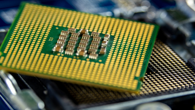
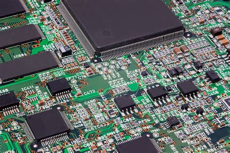
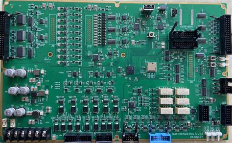
A PCB assembly (PCBA) refers to a printed circuit board populated with electronic components such as resistors, capacitors, integrated circuits (ICs), and connectors. The PCB itself provides the mechanical structure and electrical connections between components, while the assembly process ensures that all parts are correctly mounted and soldered.
Key Components of a PCB Assembly
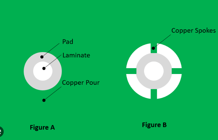
- Printed Circuit Board (PCB) – The base material, typically made of fiberglass (FR4), which contains conductive copper traces.
- Electronic Components – Includes passive components (resistors, capacitors), active components (transistors, ICs), and connectors.
- Solder – A metal alloy used to form electrical and mechanical bonds between components and the PCB.
- Silkscreen & Solder Mask – Protective layers that prevent short circuits and provide component labeling.
The PCB Assembly Process
The assembly of a PCB involves several critical steps, each requiring precision and quality control.
1. PCB Fabrication
Before assembly, the bare PCB must be manufactured. This involves:
- Design & Layout – Using CAD software to create the circuit schematic and PCB layout.
- Etching – Removing unwanted copper to form conductive traces.
- Drilling – Creating holes for through-hole components and vias.
- Layer Stacking – For multi-layer PCBs, layers are laminated together.
2. Component Placement
There are two primary methods for placing components on a PCB:
A. Surface Mount Technology (SMT)
- Components are placed directly onto the PCB surface.
- High-speed pick-and-place machines position tiny components accurately.
- Common in modern electronics due to miniaturization and efficiency.
B. Through-Hole Technology (THT)
- Components have leads inserted into drilled holes and soldered on the opposite side.
- Provides stronger mechanical bonds, used for larger components like connectors.
3. Soldering
After component placement, soldering secures the connections:
- Reflow Soldering (SMT) – The PCB passes through an oven, melting solder paste to form joints.
- Wave Soldering (THT) – The PCB moves over a wave of molten solder, bonding through-hole components.
- Hand Soldering & Rework – Used for prototypes or repairs.
4. Inspection & Testing
Quality control is crucial to ensure functionality:
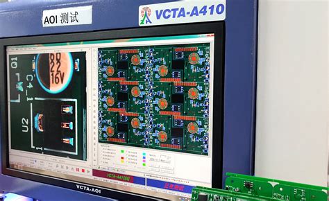
- Automated Optical Inspection (AOI) – Cameras check for misaligned or missing components.
- X-Ray Inspection – Detects hidden solder defects in Ball Grid Array (BGA) packages.
- Functional Testing – Verifies the PCB operates as intended.

Key Technologies in PCB Assembly
1. High-Density Interconnect (HDI) PCBs
- Features finer traces and smaller vias for compact, high-performance devices.
- Used in smartphones, wearables, and medical implants.
2. Flexible & Rigid-Flex PCBs
- Bendable circuits for space-constrained applications like foldable phones.
3. Internet of Things (IoT) & Embedded Systems
- PCBs in IoT devices require low power consumption and wireless connectivity.
4. Automotive & Aerospace PCBs
- Must withstand extreme temperatures, vibrations, and reliability demands.
Applications of PCB Assemblies
PCB assemblies are ubiquitous across industries:
- Consumer Electronics – Smartphones, laptops, TVs, gaming consoles.
- Medical Devices – Pacemakers, MRI machines, wearable health monitors.
- Automotive – Engine control units (ECUs), infotainment systems, ADAS.
- Industrial Automation – Robotics, sensors, control systems.
- Aerospace & Defense – Avionics, satellites, military communications.
Future Trends in PCB Assembly
1. Miniaturization & Advanced Materials
- Smaller components and high-frequency materials for 5G and AI applications.
2. Automation & AI in Manufacturing
- AI-driven defect detection and robotic assembly improve efficiency.
3. Sustainable PCB Manufacturing
- Lead-free soldering and recyclable materials reduce environmental impact.
4. 3D-Printed Electronics
- Additive manufacturing enables rapid prototyping of complex PCBs.
Conclusion
PCB assemblies are the unsung heroes of modern electronics, enabling innovation across countless industries. As technology advances, PCB manufacturing continues to evolve, embracing automation, sustainability, and cutting-edge materials. Understanding the intricacies of PCB assembly helps engineers, manufacturers, and businesses stay ahead in an increasingly connected world.