PCB Assembly and Soldering: Optimizing Quality in Electronics Manufacturing
Key Takeaways
Modern PCB assembly processes combine precision engineering with rigorous quality protocols to meet evolving industrial demands. When selecting a PCBA provider, consider their adherence to IPC-A-610 standards, which govern solder joint integrity and component placement accuracy.
"The shift toward automated optical inspection (AOI) has reduced human error by 62% in surface-mount technology (SMT) applications," notes Dr. Elena Torres, a manufacturing systems researcher.
Critical factors influencing assembly outcomes include:
| Parameter | Traditional Approach | Advanced Solution |
|---|---|---|
| Soldering Accuracy | Manual calibration | Laser-guided placement |
| Defect Detection | Visual inspection | 3D X-ray analysis |
| Thermal Management | Basic heat sinks | Phase-change materials |
For high-density interconnect (HDI) boards, reflow soldering profiles require precise temperature zoning to prevent warping. Manufacturers implementing traceability systems report 34% faster defect resolution in multilayer PCB assembly workflows.
When optimizing PCBA costs:
- Prioritize design for manufacturability (DFM) checks during prototyping
- Leverage panelization strategies to reduce material waste
- Validate thermal cycling performance for mission-critical applications
Tip: Always request first-article inspection reports to verify compliance with your project’s acceptance quality level (AQL) thresholds before full production runs.
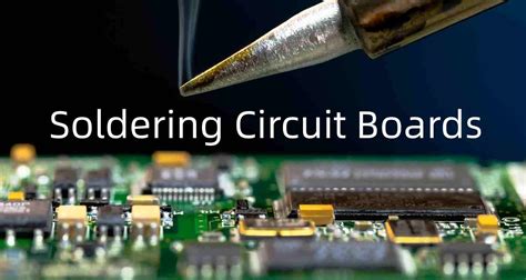
Advanced PCB Soldering Techniques
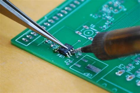
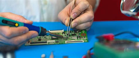
Modern PCB assembly processes rely on sophisticated soldering methods to meet the increasing demands for miniaturization and high-density interconnects. Reflow soldering remains a cornerstone technique, enabling precise solder paste application and controlled thermal profiles for components ranging from surface-mount devices (SMDs) to ball grid arrays (BGAs). For applications requiring robust mechanical bonds, wave soldering continues to excel in through-hole component integration, particularly in industrial-grade PCBA designs.
Emerging technologies like laser soldering and selective soldering are gaining traction for their ability to target specific connection points with micron-level accuracy, minimizing thermal stress on sensitive components. These methods are critical for hybrid PCB assembly projects combining rigid and flexible substrates. To ensure consistency, automated optical inspection (AOI) systems now integrate with soldering equipment, cross-verifying joint integrity against IPC-A-610 standards.
In high-reliability sectors such as aerospace or medical devices, vacuum soldering eliminates oxidation risks by operating in inert environments, a necessity for PCBA longevity. Meanwhile, advancements in lead-free solder alloys balance environmental compliance with mechanical durability, addressing RoHS directives without compromising electrical performance. By aligning these techniques with real-time process monitoring, manufacturers achieve defect rates below 50 ppm while maintaining scalability for high-volume production.
Reliable PCB Assembly Methods
Modern electronics manufacturing demands PCB assembly processes that prioritize consistency and durability. At the core of reliable PCBA workflows lies the integration of surface-mount technology (SMT) and through-hole components, which balance precision with mechanical stability. Automated pick-and-place systems ensure micron-level accuracy when positioning components, while reflow soldering techniques maintain uniform thermal profiles to prevent defects like cold joints or tombstoning.
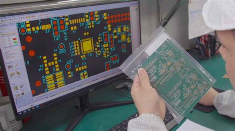
To mitigate risks in high-volume production, manufacturers employ automated optical inspection (AOI) and X-ray testing at critical stages. These steps validate solder joint integrity and component alignment, particularly for fine-pitch ICs or ball grid array (BGA) packages. Advanced PCB assembly lines also incorporate environmental controls, regulating humidity and particulate levels to protect sensitive substrates during PCBA processes.
Material selection further reinforces reliability, with lead-free solder alloys and high-temperature laminates becoming standard for industrial applications. By combining these methodologies, PCBA providers achieve <1% defect rates even in complex multilayer boards, ensuring consistent performance across automotive, aerospace, and medical devices. This systematic approach to PCB assembly creates a foundation for downstream quality assurance protocols while maintaining cost-efficiency through minimized rework.
Cost-Efficient PCB Solutions
Achieving cost efficiency in PCB assembly requires balancing economic considerations with technical precision. One proven strategy involves optimizing design layouts to minimize material waste during fabrication. By implementing Design for Manufacturing (DFM) principles, engineers can reduce unnecessary complexities, ensuring components are arranged for streamlined PCBA workflows. This approach not only lowers raw material costs but also accelerates production cycles, directly impacting overall project budgets.
Leveraging automated soldering technologies, such as reflow ovens and wave soldering systems, further enhances cost-effectiveness. These systems ensure consistent PCB assembly quality while reducing manual labor expenses, particularly in high-volume orders. Additionally, selecting standardized components over custom parts can yield significant savings without compromising functionality—a critical consideration for consumer electronics and industrial applications alike.
Strategic supplier partnerships also play a pivotal role. Bulk purchasing of substrates and solder materials, combined with Just-In-Time inventory practices, mitigates storage costs and material obsolescence risks. For startups and scaled enterprises, outsourcing PCBA to certified manufacturers with tiered pricing models often provides flexibility, allowing businesses to align expenses with production demands.
By integrating these methods, manufacturers maintain competitive pricing while adhering to rigorous quality benchmarks—a foundation for succeeding in markets where reliability and affordability are equally prioritized.
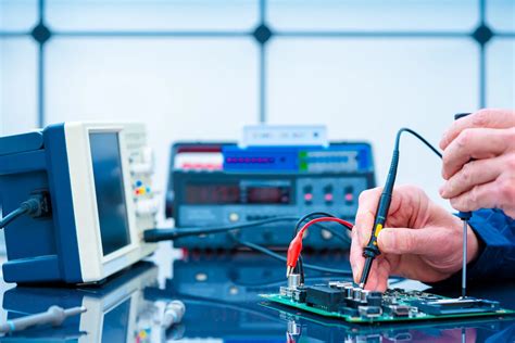
PCB Quality Control Standards
Implementing rigorous PCB assembly quality control protocols is essential for ensuring the reliability and longevity of electronic devices. Modern pcb assembly and soldering services adhere to internationally recognized standards such as IPC-A-610 (Acceptability of Electronic Assemblies) and IPC-J-STD-001 (Requirements for Soldered Electrical Connections), which define criteria for solder joint integrity, component placement accuracy, and material compatibility. Automated optical inspection (AOI) systems and X-ray testing are routinely deployed during PCBA processes to detect microscopic defects like cold solder joints, tombstoning, or misaligned components that could compromise functionality.
To maintain consistency, manufacturers employ statistical process control (SPC) methods, tracking metrics such as solder paste volume uniformity and reflow oven temperature profiles. For high-reliability applications—including aerospace or medical devices—additional testing like environmental stress screening (ESS) and accelerated life testing validates performance under extreme conditions. Cross-functional teams often conduct failure mode and effects analysis (FMEA) to preemptively address risks in PCB assembly workflows.
By integrating these standards with real-time data analytics, pcb assembly and soldering services achieve defect rates below 0.1%, ensuring compliance with both industrial specifications and end-user expectations. This systematic approach not only reduces rework costs but also reinforces the reputation of PCBA providers as partners in delivering mission-critical electronics.
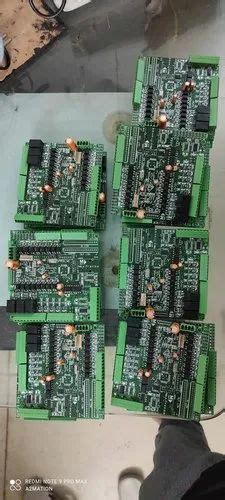
Industrial PCB Applications
In industrial environments, PCB assembly (PCBA) processes must meet rigorous operational demands across sectors like automotive, aerospace, and medical device manufacturing. These applications require boards capable of withstanding extreme temperatures, mechanical stress, and prolonged operational cycles. For example, automotive control systems rely on vibration-resistant PCBA designs to ensure stability in harsh driving conditions, while aerospace electronics demand ultra-precise soldering to maintain functionality at high altitudes.
Industrial-grade PCB assembly prioritizes material selection, with substrates like polyimide or ceramic composites enhancing thermal management and durability. Advanced soldering techniques, such as selective laser soldering, enable consistent joints in high-density layouts common in industrial robotics or power distribution systems. Quality assurance protocols, including automated optical inspection (AOI) and X-ray testing, verify compliance with IPC-A-610 standards, minimizing defects in mission-critical applications.
From factory automation to renewable energy infrastructure, industrial PCBA solutions balance performance with scalability. Manufacturers often integrate modular designs to simplify repairs or upgrades, reducing downtime in production lines. As industries adopt smarter technologies, the role of robust PCB assembly and soldering services becomes pivotal in maintaining seamless integration between hardware and IoT-enabled systems.
Automated Soldering Innovations
The evolution of PCB assembly processes has been revolutionized by advancements in automated soldering technologies, which combine precision engineering with intelligent systems to address modern manufacturing challenges. Robotic soldering systems equipped with vision-guided positioning now achieve micron-level accuracy, ensuring consistent joint formation across high-density PCBA designs. These systems leverage machine learning algorithms to adapt to component variations in real time, minimizing defects in complex layouts such as ball grid arrays (BGAs) or quad flat no-lead (QFN) packages.
A key breakthrough lies in laser soldering and selective soldering techniques, which enable localized heat application to prevent thermal stress on sensitive components. This is particularly critical for mixed-technology boards combining surface-mount (SMT) and through-hole components. Manufacturers integrating inline automated optical inspection (AOI) systems within PCB assembly lines have reduced error rates by 40-60% compared to manual checks, according to IPC-610 benchmarking studies.
The shift toward closed-loop process control further enhances reliability, with sensors continuously monitoring parameters like solder paste viscosity and reflow oven temperature gradients. Such innovations not only accelerate production throughput but also support zero-defect manufacturing initiatives essential for aerospace and medical PCBA applications. As these technologies mature, their convergence with IoT-enabled predictive maintenance is setting new benchmarks for yield optimization in high-volume electronics production.
Consumer Electronics Soldering
The demand for precision in PCB assembly for consumer electronics has intensified as devices shrink in size while growing in complexity. Surface-mount technology (SMT) remains pivotal, enabling the placement of microscopic components like 0402 resistors or QFN packages onto densely layered boards. Modern PCBA workflows integrate automated optical inspection (AOI) systems to detect solder bridges or cold joints, which are critical flaws in high-volume production of smartphones, wearables, and IoT gadgets.
To balance speed and accuracy, manufacturers employ reflow soldering profiles tailored to lead-free alloys, ensuring compliance with RoHS directives without compromising joint integrity. For flexible circuits found in foldable displays or compact sensors, selective soldering techniques minimize thermal stress on sensitive substrates. Rigorous testing protocols, including functional circuit validation and environmental stress screening, verify that consumer-grade electronics withstand real-world usage patterns—from temperature fluctuations to mechanical wear.
As consumer expectations evolve, PCB assembly providers prioritize traceability systems to track component origins and soldering parameters, aligning with global quality benchmarks. This focus on repeatable processes not only reduces defects but also supports scalable, cost-effective manufacturing—a necessity in markets where margins tighten as innovation accelerates.
Future PCB Manufacturing Trends
As the electronics industry evolves, PCB assembly processes are undergoing transformative shifts driven by Industry 4.0 integration and sustainability demands. Smart factories leveraging AI-driven analytics and IoT-enabled monitoring are redefining PCBA workflows, enabling real-time defect detection and predictive maintenance. Advanced robotics, paired with machine learning algorithms, now optimize soldering precision while minimizing material waste—a critical advancement for high-volume production environments.
Another critical development is the adoption of additive manufacturing techniques, such as 3D-printed circuitry, which streamline prototyping cycles and support complex, multi-layer designs. These innovations align with growing requirements for miniaturization in consumer electronics and high-reliability components for aerospace applications.
Sustainability is also reshaping PCB assembly, with manufacturers prioritizing lead-free soldering alloys and recyclable substrates. Emerging closed-loop systems aim to recover precious metals from discarded boards, reducing environmental impact without compromising performance.
Looking ahead, hybrid production models—combining automated PCBA lines with flexible, small-batch capabilities—will dominate, catering to both mass-market demands and specialized industrial needs. This dual approach ensures cost-efficiency while maintaining agility in an increasingly dynamic market.
Conclusion
In the evolving landscape of electronics manufacturing, PCB assembly and PCBA processes remain foundational to delivering high-performance devices. By integrating automated soldering technologies and rigorous inspection protocols, manufacturers achieve a critical balance between precision and cost-effectiveness. The emphasis on traceability and thermal management ensures that industrial-grade systems and consumer electronics alike meet stringent reliability standards.
As demand grows for smarter, smaller, and more energy-efficient products, partnerships with PCB assembly providers become pivotal. These collaborations enable brands to leverage scalable solutions while maintaining compliance with international quality frameworks. Looking ahead, advancements in AI-driven defect detection and lead-free soldering materials will further refine production workflows, reducing waste and accelerating time-to-market.
Ultimately, the success of modern electronics hinges on harmonizing innovation with meticulous execution in PCBA stages. By prioritizing adaptability and continuous improvement, manufacturers can navigate shifting market demands while upholding the integrity of every circuit board produced.
FAQs
What quality control measures ensure reliability in PCB assembly?
Advanced PCBA processes integrate automated optical inspection (AOI) and X-ray testing to detect soldering defects, component misalignment, and micro-cracks. These systems validate compliance with IPC-A-610 standards, crucial for mission-critical applications like medical devices or aerospace systems.
How do soldering techniques impact manufacturing costs?
Selective soldering and reflow ovens optimize material usage while reducing thermal stress on components. By pairing these methods with design for manufacturability (DFM) principles, producers achieve 30-45% faster cycle times without compromising joint integrity in high-density PCB assemblies.
What distinguishes prototype assembly from mass production?
Prototype PCBA focuses on functional validation using rapid-turn services, while volume manufacturing emphasizes process repeatability. Both stages require temperature-controlled soldering profiles to prevent pad lifting or cold joints, particularly in lead-free RoHS-compliant builds.
Can automated systems handle complex mixed-technology boards?
Modern PCB assembly lines combine robotic SMT placement with precision through-hole insertion, accommodating boards featuring 0201 components alongside high-power connectors. Vision-guided systems achieve ±25μm placement accuracy, essential for 5G infrastructure and automotive control modules.
How are evolving sustainability standards shaping soldering processes?
The transition to halogen-free fluxes and recyclable solder alloys aligns with global environmental directives. Leading PCBA providers now implement closed-loop solder recovery systems, reducing waste generation by 60-70% compared to conventional rework stations.
Optimize Your Electronics Production Today
For tailored PCB assembly and soldering solutions that balance precision with scalability, please click here to consult our engineering team.


