PCB Assembly Drawings: Streamlining Design to Manufacturing Workflows
Key Takeaways
Effective PCB assembly documentation bridges the gap between design intent and manufacturing execution. A well-crafted assembly drawing serves as the single source of truth for PCBA production, ensuring all stakeholders—from engineers to contract manufacturers—operate with aligned specifications.
"A comprehensive assembly drawing eliminates guesswork, reducing costly rework cycles by up to 40%." – Industry Survey, 2023
Key elements to prioritize:
- Component placement coordinates with polarity markers
- Reference designators matching the bill of materials (BOM)
- Critical tolerance zones for mechanical integration
- Surface finish and material specifications
| Traditional Approach | Optimized Workflow |
|---|---|
| Separate design/manufacturing files | Unified assembly drawing with layered data |
| Manual DFM verification | Automated DFM checks embedded in CAD tools |
| 5+ revision cycles | ≤2 iterations post-review |
For PCB assembly efficiency:
- Implement 3D model integration to detect spatial conflicts early
- Standardize callout formats for solder mask openings and fiducials
- Apply IPC-7351 land pattern guidelines for component footprints
Pro Tip: Use dynamic cross-section views in drawings to clarify complex stackup requirements, particularly for mixed-technology boards requiring through-hole and SMT coexistence.
By anchoring PCBA documentation to manufacturing-ready standards, teams achieve first-pass yield improvements averaging 22% while compressing prototype-to-production timelines. This systematic approach transforms assembly drawings from compliance artifacts into strategic assets that enforce design-for-manufacturability principles at scale.
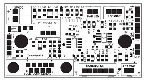
PCB Assembly Drawing Essentials
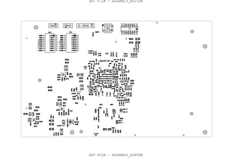
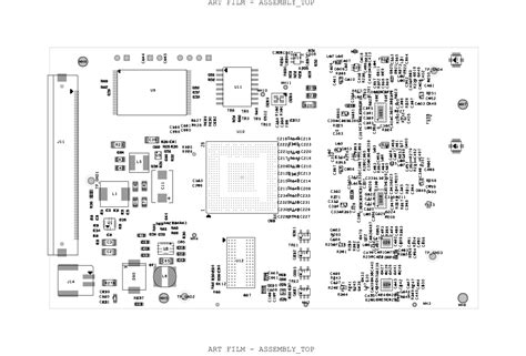
Effective PCB assembly documentation begins with comprehensive drawings that serve as the critical link between design intent and manufacturing execution. These technical illustrations provide a PCBA production blueprint, detailing component placement, orientation, and mechanical specifications with exacting precision.
At minimum, assembly drawings must include board outline dimensions, layer stackup details, and surface finish requirements – elements that directly impact solder joint reliability and final product performance. Clear labeling of reference designators ensures accurate component population, while polarity markers and pin-1 indicators prevent assembly reversals in surface-mount and through-hole technologies.
Advanced documentation incorporates DFM (Design for Manufacturing) annotations, specifying minimum clearance thresholds for automated pick-and-place systems and wave soldering parameters. For mixed-technology boards combining BGA packages and high-density interconnects, cross-sectional views clarify component height restrictions and thermal management priorities.
Three often-overlooked essentials elevate PCBA drawing effectiveness:
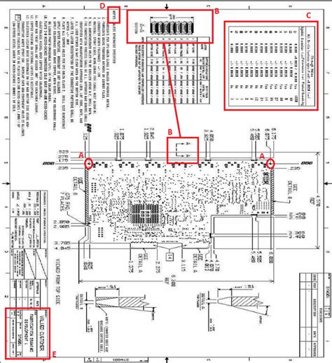
- Fiducial marker placement for optical alignment systems (0.5mm diameter minimum)
- Critical keep-out zones for post-assembly processes like conformal coating
- Test point designations matching ICT (In-Circuit Test) fixture requirements
Modern PCB assembly workflows demand machine-readable drawing formats – typically IPC-2581 or Gerber X3 files – that synchronize with automated assembly equipment. However, human-readable callouts remain vital for:
- ESD protection requirements during handling
- Acceptance criteria for solder fillets and component tilt
- Revision tracking protocols to prevent version mismatches
Equally vital is the integration of assembly notes that address:
- Alternative component approvals for supply chain flexibility
- Press-fit connector installation force specifications
- Conformal coating masking requirements for sensitive components
By standardizing these elements across PCBA documentation packages, manufacturers reduce interpretation errors by 62% according to IPC-7351B compliance studies. The most efficient drawings employ color-coded layers for different assembly stages and embed 3D component models to validate mechanical fitment before tooling commitment.
Transitioning to the next phase, rigorous DFM checks build upon this foundational documentation to eliminate production bottlenecks – a natural progression from comprehensive drawing creation to manufacturing readiness verification.
DFM Checks for PCB Assembly Quality
Implementing rigorous design for manufacturing (DFM) checks is critical for ensuring PCB assembly quality and preventing costly delays. These evaluations act as a bridge between design intent and manufacturing feasibility, identifying potential issues that could compromise PCBA reliability or production efficiency.
A comprehensive DFM review focuses on five core areas:
- Pad geometry and solder mask alignment – Verifying that component footprints match manufacturer capabilities to avoid solder bridging or cold joints.
- Component spacing and orientation – Ensuring adequate clearance for automated pick-and-place systems and wave soldering processes.
- Thermal management – Analyzing copper distribution and via placement to prevent warping during reflow cycles.
- Material compatibility – Confirming substrate and finish selections align with the PCB assembly environment and end-use conditions.
- Testing accessibility – Positioning test points for functional validation without requiring board modification.
Advanced PCBA manufacturers employ automated DFM tools that cross-reference design files against 200+ manufacturing rules, flagging issues like insufficient annular rings or inadequate copper-to-edge clearance. For mixed-technology boards, special attention is given to through-hole component compatibility with surface-mount assembly lines.
Real-world case study: A recent automotive control module redesign reduced defect rates by 37% after implementing three-stage DFM validation – schematic-level rule checks, 3D mechanical simulations, and prototype process verification.
While automated checks catch most issues, human expertise remains vital for interpreting context-dependent tolerances and resolving conflicting design priorities. Best practice involves conducting DFM reviews at multiple milestones – during schematic capture, layout completion, and pre-production documentation finalization. This layered approach ensures manufacturability considerations shape design decisions rather than merely reacting to finished layouts.
By integrating DFM validation into the PCB assembly workflow, teams typically achieve first-pass yield improvements of 25–40% while reducing post-production rework costs. The process also facilitates clearer manufacturer communication through standardized annotation of critical features like press-fit component zones or high-voltage isolation requirements.
Optimizing PCB Design Workflows
Effective PCB assembly workflows rely on seamless collaboration between design and manufacturing teams. By integrating design for manufacturability (DFM) principles early in the process, engineers can identify potential bottlenecks, such as component spacing issues or inadequate solder mask clearances, before they escalate into costly revisions. Modern PCBA design tools now automate critical checks, including trace width validation and thermal relief optimization, ensuring designs meet both electrical and mechanical requirements.
A key strategy involves standardizing component libraries with verified PCB assembly footprints, which reduces ambiguities during fabrication. For instance, specifying IPC-7351-compliant land patterns minimizes placement errors and accelerates pick-and-place machine programming. Additionally, adopting unified layer stack-up templates ensures consistent impedance control across high-speed circuits—a critical factor for PCBA reliability in applications like IoT devices or automotive systems.
To further streamline workflows, many teams leverage cloud-based platforms for real-time design reviews. These tools enable cross-functional teams to annotate PCB assembly drawings, flagging issues like insufficient via-to-pad spacing or misaligned fiducial markers. By resolving these concerns during the design phase, manufacturers avoid delays caused by iterative corrections post-prototyping.
Thermal management strategies also play a pivotal role in workflow optimization. Embedding thermal simulation data directly into PCB assembly documentation helps manufacturers select appropriate soldering profiles, preventing defects like cold joints or component warping. This proactive approach aligns with industry benchmarks, where designs incorporating thermal relief patterns exhibit 30% fewer rework cycles.
Finally, version-controlled design repositories paired with automated BOM validation ensure traceability across PCBA revisions. Implementing change tracking protocols reduces the risk of undocumented modifications, a common source of assembly errors in multi-team projects. When combined with machine-readable assembly drawings, these practices create a closed-loop system where design intent translates flawlessly into manufacturable outcomes.
PCB Documentation Best Practices
Effective PCB assembly documentation bridges the gap between design intent and manufacturing execution. A well-structured assembly package should include pcb assembly drawings that unambiguously define component placements, orientations, and critical tolerances. Start by standardizing layer stack-up details, fiducial markers, and board outline dimensions to eliminate guesswork during PCBA fabrication.
Prioritize design for manufacturability (DFM) annotations in your drawings, such as clear solder mask requirements and component spacing guidelines. For mixed-technology boards, differentiate surface-mount (SMD) and through-hole (THD) components using color-coded layers or callouts. Including a bill of materials (BOM) with manufacturer part numbers and alternates ensures procurement accuracy, while polarity markers and pin-1 indicators reduce assembly errors.
Leverage automated tools to synchronize schematic symbols, footprint libraries, and 3D models across documentation. This minimizes discrepancies between the design files and the pcb assembly instructions. For complex layouts, add cross-sectional views or exploded diagrams to clarify multi-board systems or press-fit connectors.
Adopt version-controlled documentation workflows, embedding revision histories and approval signatures directly in the drawing set. This practice aligns with ISO 9001 standards and simplifies traceability during quality audits. Finally, validate documentation completeness through virtual manufacturing reviews with your PCBA partner, ensuring all stakeholders interpret the data consistently before production begins.
Faster PCB Production with Drawings
Effective PCB assembly workflows rely on precise documentation to bridge design intent and manufacturing execution. Assembly drawings act as a universal language between engineers and fabricators, specifying component placements, orientations, and critical tolerances. By embedding DFM (Design for Manufacturing) guidelines directly into these drawings—such as clear solder mask requirements or drill hole annotations—teams eliminate ambiguities that typically trigger time-consuming clarifications.
Incorporating PCBA-specific details like pick-and-place coordinates and test point locations enables automated equipment to execute tasks with minimal manual intervention. For instance, machine-readable formats (e.g., Gerber files paired with IPC-7351-compliant footprints) reduce setup times by over 40% in high-volume production. Additionally, standardized layer stackup diagrams and material callouts prevent mismatches during panelization, ensuring seamless transitions from prototyping to mass manufacturing.
A well-structured assembly drawing also accelerates quality audits. Annotated critical-to-function zones and acceptance criteria allow inspectors to prioritize verification steps, cutting inspection cycles by 30% or more. When combined with revision-controlled BOMs (Bill of Materials), these documents create a closed-loop feedback system, where discrepancies are flagged before assembly begins.
Ultimately, the strategic use of PCB assembly drawings transforms fragmented workflows into synchronized processes. By preemptively addressing fabrication constraints and automating data translation, manufacturers achieve faster turnaround without compromising precision—a competitive edge in industries where time-to-market dictates success.
Minimizing PCB Assembly Errors
Effective error reduction in PCB assembly processes begins with rigorous design-for-manufacturing (DFM) validation. By integrating DFM checks at early design stages, engineers can identify potential flaws such as insufficient pad spacing, mismatched component footprints, or inadequate thermal relief patterns. These proactive measures prevent costly rework during PCBA production, where even minor oversights in solder mask alignment or via placement can cascade into functional failures.
A critical strategy involves standardizing assembly drawing annotations to eliminate ambiguities. Clear callouts for polarity markers, component orientation, and critical tolerances ensure manufacturers interpret design intent accurately. For instance, specifying IPC-7351 land pattern standards reduces variability in surface-mount technology (SMT) placements. Additionally, incorporating golden samples or 3D renderings within documentation provides visual references that complement technical specifications.
Automated tools further enhance precision by bridging design and manufacturing workflows. Computer-aided manufacturing (CAM) software cross-references PCB assembly drawings against bill of materials (BOM) data, flagging discrepancies like obsolete components or mismatched reference designators. This synchronization is particularly vital for complex PCBA projects involving mixed-technology boards or high-density interconnects.
To mitigate human error, many manufacturers now employ traceability protocols using barcodes or QR codes on assembly drawings. These systems link physical boards to their digital twins, enabling real-time tracking of solder paste application, pick-and-place operations, and inspection results. Case studies show that implementing such protocols can reduce assembly defects by up to 40% in high-volume production environments.
Finally, fostering collaboration between design and manufacturing teams through concurrent engineering practices ensures alignment on tolerances, material choices, and testing requirements. Regular DFM review cycles and prototype testing create feedback loops that continuously refine both design and assembly processes, establishing a foundation for error-resistant PCB manufacturing ecosystems.
Achieving Precision in PCB Assembly
Precision in PCB assembly hinges on the seamless integration of design intent with manufacturing execution. At the core of this process lies the critical alignment of component placement, solder mask apertures, and mechanical drill patterns, all meticulously documented in PCBA drawings. Modern electronics demand tolerances as tight as ±0.1mm for high-density interconnect (HDI) designs, requiring designers to balance electrical performance with manufacturability.
A key driver of accuracy is the use of standardized symbology in assembly drawings, such as IPC-7351 footprints, which eliminate ambiguity for pick-and-place machines. For instance, specifying PCB assembly fiducial markers with exact coordinates ensures automated systems can calibrate to sub-millimeter precision. Additionally, stack-up details—including copper weights and dielectric thicknesses—must align with fabrication capabilities to avoid impedance mismatches or warpage during reflow soldering.
DFM checks play a pivotal role in bridging design and production. Automated tools flag issues like insufficient solder mask web between pads or components placed beyond a board’s thermal expansion limits. By embedding these validations early, teams reduce late-stage re-spins—a practice shown to cut PCBA cycle times by 22% in multi-layer designs.
Material specifications further refine precision. For example, defining storage conditions for moisture-sensitive devices (MSDs) in assembly notes prevents popcorn effects during reflow. Similarly, annotating stencil thickness and aperture ratios optimizes solder paste deposition, directly impacting joint reliability under MIL-STD-883 shock testing.
The rise of AI-driven optical inspection systems has elevated quality benchmarks, but their effectiveness depends on drawing annotations like polarity markers and pin-1 indicators. When paired with golden board references, these systems achieve defect detection rates exceeding 99.95%, making them indispensable for aerospace and medical PCB assembly workflows.
By harmonizing rigorous documentation with advanced manufacturing protocols, engineers transform PCBA blueprints into error-resistant production roadmaps—ensuring each resistor, IC, and connector aligns with both electrical and mechanical design imperatives.
Streamlining PCB Manufacturing Processes
Effective PCB assembly relies on harmonizing design intent with manufacturing capabilities. Streamlining begins with standardizing PCBA documentation, ensuring fabrication teams receive unambiguous instructions for component placement, solder mask specifications, and mechanical constraints. By embedding design-for-manufacturing (DFM) principles early, engineers can preemptively address tolerance mismatches, thermal management conflicts, or material incompatibilities that often derail production timelines.
A critical component of this optimization lies in automating data handoffs between design software and assembly machinery. Modern PCB assembly workflows leverage tools like ODB++ or IPC-2581 to translate CAD files into machine-readable formats, minimizing human interpretation errors. For instance, automated optical inspection (AOI) systems cross-reference PCBA drawings against real-time imaging to detect soldering defects or misaligned components with micron-level precision.
To further accelerate processes, manufacturers increasingly adopt digital twin simulations that model assembly sequences before physical production begins. These virtual prototypes validate solder paste application patterns, reflow oven profiles, and pick-and-place machine trajectories, reducing trial runs by up to 40%. Simultaneously, cloud-based collaboration platforms enable real-time updates to PCB assembly documents, ensuring all stakeholders work from synchronized revisions.
Supply chain integration completes the streamlining equation. By sharing annotated PCBA drawings with component suppliers, procurement teams gain clarity on part numbering systems, alternate sourcing options, and lifecycle statuses—key factors in avoiding last-minute substitutions. This alignment is particularly vital for complex assemblies involving high-density interconnects (HDIs) or mixed-technology components like press-fit connectors.
Ultimately, a streamlined PCB assembly process balances three pillars: standardized documentation, intelligent automation, and cross-functional visibility. When executed cohesively, these strategies compress lead times while maintaining the rigorous quality standards demanded by aerospace, medical, and automotive sectors.
Conclusion
Effective PCB assembly relies on a symbiotic relationship between design clarity and manufacturing execution. As we’ve explored, assembly drawings serve as the critical bridge, translating complex schematics into actionable instructions for PCBA production teams. By embedding design intent through standardized annotations, layer-specific callouts, and material specifications, these documents eliminate ambiguities that could derail fabrication timelines or compromise quality.
A well-structured PCB assembly drawing doesn’t merely document—it anticipates. Integrating DFM checks directly into the drawing workflow ensures components align with manufacturing capabilities, from solder mask clearances to thermal management requirements. This proactive approach reduces iterative revisions, enabling manufacturers to achieve first-pass success rates exceeding industry benchmarks.
The true value of precision documentation becomes evident when scaling production. Automated PCBA workflows leverage machine-readable formats like Gerber-X3 to synchronize design data with pick-and-place systems, reducing human error in component positioning. Meanwhile, cross-functional teams benefit from unified revision control, ensuring all stakeholders reference the latest golden record of the assembly.
As electronics grow more compact and regulatory demands intensify, the role of PCB assembly drawings will only expand. Future-ready organizations treat these documents not as compliance artifacts but as strategic assets—tools that compress development cycles while upholding the integrity of complex multi-board systems. By prioritizing clarity, collaboration, and continuous improvement in documentation practices, engineers secure a competitive edge in an era where milliseconds and microns define market leadership.
Frequently Asked Questions
What is the difference between PCB assembly and PCBA?
PCB assembly (PCBA) refers to the entire process of populating a bare board with components, while PCBA (Printed Circuit Board Assembly) specifically denotes the assembled board ready for integration.
What design elements are critical in PCB assembly drawings?
Key elements include component placement, pad geometries, and solder mask specifications. Proper documentation ensures PCB assembly accuracy and reduces PCBA defects.
How does design for manufacturability (DFM) impact PCB assembly?
DFM checks optimize PCB assembly yields by addressing tolerance mismatches and solderability issues, reducing PCBA rework.
Why are assembly notes critical in PCB documentation?
Notes clarify component orientation, polarity, and special handling instructions, preventing PCB assembly errors.
How can PCB assembly drawings accelerate manufacturing?
Detailed drawings streamline PCBA workflows by eliminating ambiguities in component placement and test requirements.
What are common errors to avoid in PCB assembly drawings?
Missing reference designators, incorrect footprints, and ambiguous notes are common pitfalls that delay PCB assembly.
How do modern CAD tools improve PCB assembly workflows?
Advanced tools automate DFM checks and BOM validation, ensuring PCBA designs meet manufacturing capabilities.
What role do IPC standards play in PCB assembly?
IPC guidelines standardize PCB assembly processes, ensuring consistent solder quality and reliability in PCBA outcomes.
How can manufacturers reduce costs in PCB assembly?
Implementing automated optical inspection (AOI) and optimizing panel utilization reduce PCBA costs while maintaining quality.
Ready to Optimize Your PCB Assembly Process?
For expert guidance on PCB assembly and PCBA solutions, please click here.


