PCB Assembly Essentials for Reliable Electronics
Key Takeaways
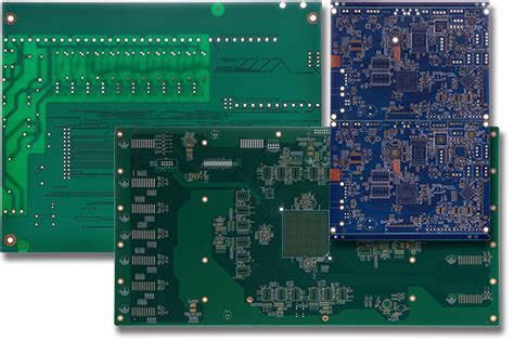
Successful PCB assembly hinges on balancing design precision, material science, and manufacturing rigor. For PCBA (Printed Circuit Board Assembly) to deliver reliability in demanding applications, engineers must prioritize design for manufacturability (DFM) principles, ensuring layouts accommodate automated soldering and inspection workflows. Critical considerations include:
| Factor | Impact on Reliability | Best Practices |
|---|---|---|
| Component Placement | Reduces soldering defects | Align with pick-and-place machine tolerances |
| Thermal Management | Prevents overheating failures | Use thermal vias and heatsinks in dense layouts |
| Material Compatibility | Avoids delamination under stress | Match substrate Tg rating to operating conditions |
Robustness begins with selecting components rated for operational extremes—temperature, vibration, and humidity—while soldering techniques like reflow or wave soldering must align with pad geometries and alloy properties. Post-assembly, automated optical inspection (AOI) and X-ray testing validate solder joint integrity, particularly for hidden connections in ball grid arrays (BGAs). For mission-critical systems, accelerated life testing (ALT) simulates years of stress within days, uncovering latent flaws. By integrating these strategies, PCB assembly transitions from a manufacturing step to a reliability engineering discipline.
PCB Design Principles for Reliable Assembly
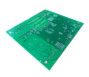
Effective PCB assembly begins with design choices that prioritize manufacturability and long-term performance. A well-optimized layout minimizes electromagnetic interference (EMI) risks while ensuring pcba compatibility with automated production lines. Critical considerations include maintaining adequate trace spacing to prevent solder bridging and incorporating thermal relief patterns for components prone to heat stress during soldering.
Designers must align pad geometries with surface-mount technology (SMT) specifications, particularly for fine-pitch ICs or ball grid array (BGA) packages. Implementing teardrop transitions at trace-to-pad junctions enhances mechanical stability, reducing fracture risks in high-vibration environments. For mixed-technology boards combining SMT and through-hole components, strategic component grouping streamlines both pcb assembly workflows and post-soldering inspections.
Material selection directly impacts reliability: high-Tg laminates (170°C+) prevent delamination in thermal cycling, while proper copper weight balancing ensures consistent impedance control. Adherence to IPC-2221 standards for annular ring sizing and via placement prevents lift-off defects during reflow processes. By integrating Design for Manufacturing (DFM) checks early in the layout phase, engineers mitigate rework costs and accelerate time-to-market for mission-critical pcba applications. This foundation supports subsequent stages, from precision soldering to rigorous testing protocols.
Component Selection Criteria for Robust PCBs
Selecting components for PCB assembly requires balancing performance, durability, and manufacturability. Start by prioritizing environmentally rated parts, such as those meeting IPC-610 Class 3 standards, to ensure reliability in demanding conditions. Components with higher temperature tolerances (e.g., -55°C to 125°C) and moisture resistance reduce failure risks in harsh environments.
When sourcing for PCBA, verify manufacturer certifications—ISO 9001 or IATF 16949 compliance indicates rigorous quality control. Opt for surface-mount devices (SMDs) with standardized footprints to simplify automated placement and minimize soldering defects. For mission-critical applications, derating practices—using components below their maximum ratings—extend operational lifespans.
Material compatibility is equally critical. Pair ceramic capacitors with low-thermal-resistance substrates to manage thermal stress, and avoid mixing metallic finishes (e.g., HASL with ENIG) that may cause intermetallic issues. Additionally, select connectors with robust mating cycles and corrosion-resistant coatings to maintain signal integrity.
Finally, validate component choices through accelerated life testing and thermal cycling simulations. This proactive approach identifies weaknesses before mass production, aligning with PCB assembly quality benchmarks like IPC-A-610. By integrating these criteria, designers ensure the PCBA delivers consistent performance across its lifecycle.
Soldering Techniques Ensuring Electrical Integrity
Effective soldering forms the cornerstone of reliable PCB assembly, directly impacting electrical continuity and long-term performance. In PCBA manufacturing, reflow soldering remains the gold standard for surface-mount devices (SMDs), requiring precise thermal profiling to achieve uniform melting without component degradation. For through-hole components, wave soldering demands meticulous control of solder bath temperature and conveyor speed to prevent void formation or cold joints.
Advanced techniques like selective soldering address mixed-technology boards, isolating heat-sensitive components while ensuring robust connections. Implementing nitrogen-assisted soldering minimizes oxidation, enhancing solder joint integrity—a critical factor for high-frequency or high-power applications. Post-soldering, automated optical inspection (AOI) verifies joint geometry, while X-ray inspection detects hidden defects like head-in-pillow anomalies in BGA packages.
Modern PCB assembly workflows integrate real-time thermal monitoring to maintain ±2°C accuracy across heating zones, preventing thermal shock that could compromise laminate adhesion. For mission-critical assemblies, cross-sectional analysis validates solder fillet penetration, ensuring compliance with IPC-A-610 Class 3 standards. These protocols, when combined with flux chemistry optimization, create durable intermetallic bonds capable of withstanding mechanical stress and thermal cycling in harsh operational environments.
Automated Inspection Methods for Quality Assurance
Modern PCB assembly processes rely heavily on automated inspection systems to maintain consistent quality in high-volume production. Automated Optical Inspection (AOI) uses high-resolution cameras and machine vision algorithms to detect surface-level defects such as solder bridging, component misalignment, or missing parts. For hidden connections in complex PCBA designs, X-ray Inspection (AXI) provides non-destructive analysis of ball grid arrays (BGAs) and through-hole solder joints, identifying voids or cracks invisible to optical systems.
Tip: Combine AOI with in-circuit testing (ICT) to cross-verify functional performance and physical assembly quality.
Advanced systems integrate artificial intelligence to refine defect recognition accuracy, reducing false positives by learning from historical production data. In mission-critical applications, 3D solder paste inspection (SPI) ensures precise deposition volume and alignment before component placement, preventing rework costs. These methods achieve detection rates exceeding 99.9% for common PCB assembly flaws, compared to 85-90% with manual checks.
As PCBA designs shrink in size but grow in complexity, automated cross-section analysis becomes vital for validating multilayer board integrity. Thermal imaging modules can also flag overheating risks in real-time during functional testing. By synchronizing inspection data with assembly line controls, manufacturers enable closed-loop process optimization – a critical capability for automotive and aerospace-grade electronics requiring zero-defect outcomes.
Thermal Management in Dense PCB Layouts
Effective heat dissipation becomes paramount in PCB assembly designs where component density compromises airflow and conductive pathways. Modern high-power applications demand strategic placement of thermal vias beneath heat-generating components like processors or voltage regulators, creating vertical channels to transfer energy to inner copper layers or external heatsinks. In PCBA designs, selecting materials with optimal thermal conductivity coefficients—such as metal-core substrates or ceramic-filled laminates—proactively mitigates hot-spot formation.
Advanced layout techniques integrate copper pour areas with calculated clearance to balance electromagnetic compatibility (EMC) and thermal performance. Designers often employ simulation tools to model heat distribution patterns, adjusting component spacing and trace widths to prevent thermal stress on solder joints. For mission-critical systems, active cooling solutions—including micro-fans or thermoelectric coolers—are paired with conformal coatings to maintain operational stability in constrained environments.
Quality-focused PCB assembly processes validate thermal strategies through infrared thermography and accelerated aging tests, ensuring sustained reliability under peak thermal loads. This systematic approach to thermal management in PCBA workflows directly correlates with extended product lifespans, particularly in automotive or industrial electronics where temperature fluctuations exceed standard operating thresholds.
Conformal Coating Applications for Harsh Environments
In demanding operating conditions, PCB assembly reliability hinges on effective protection against environmental stressors. Conformal coatings serve as a critical barrier, shielding circuits from moisture, dust, chemical exposure, and thermal cycling—common challenges in automotive, aerospace, and industrial applications. Selecting the right coating material—such as acrylic, silicone, or urethane—depends on factors like operating temperature ranges, flexibility requirements, and chemical resistance. For instance, silicone-based coatings excel in high-temperature environments, while polyurethane offers superior abrasion resistance.
Automated PCBA processes often integrate selective coating systems to ensure precise application, avoiding components like connectors or heat sinks that require direct exposure. Proper curing cycles and thickness control (typically 25–75 μm) are vital to prevent delamination or compromised electrical performance. Engineers must also validate coating integrity through tests like humidity resistance (per IPC-CC-830 standards) and thermal shock simulations. By aligning material properties with application-specific risks, conformal coatings extend the operational lifespan of assemblies in harsh settings, complementing earlier design and soldering quality measures.
Testing Protocols for Mission-Critical Electronics
In PCB assembly for mission-critical systems, rigorous testing protocols form the backbone of reliability. These systems, deployed in aerospace, medical, or industrial automation, demand PCBA validation that exceeds standard functional checks. A layered approach begins with automated optical inspection (AOI) to detect soldering defects like bridging or insufficient joints, followed by X-ray inspection for hidden issues in ball grid arrays (BGAs) or multilayer boards.
Environmental stress testing simulates extreme conditions—thermal cycling (-55°C to 125°C), vibration, and humidity exposure—to ensure material compatibility and solder joint integrity. For high-reliability applications, boundary scan testing validates complex interconnects, while in-circuit testing (ICT) verifies component-level performance against design specifications.
Mission-critical PCB assembly also incorporates failure mode and effects analysis (FMEA) to preemptively address risks. Advanced labs employ burn-in testing, operating boards at elevated voltages and temperatures to accelerate latent failures. Compliance with standards like IPC-A-610 (Class 3) and MIL-STD-883 ensures traceability and repeatability, critical for industries where mean time between failures (MTBF) directly impacts safety. By integrating these protocols, manufacturers mitigate risks in PCBA destined for environments where downtime is not an option.
Material Compatibility in Advanced PCB Assembly
Selecting compatible materials forms the cornerstone of reliable PCB assembly, particularly in high-performance applications where thermal, mechanical, and chemical stressors are prevalent. Advanced PCBA workflows demand rigorous evaluation of substrate materials, solder alloys, and protective coatings to prevent delamination, galvanic corrosion, or thermal expansion mismatches. For instance, combining high-temperature laminates like polyimide with lead-free solders requires precise matching of coefficients of thermal expansion (CTE) to avoid joint fractures during thermal cycling.
Modern designs increasingly incorporate mixed-material stacks, blending FR-4 substrates with ceramic-filled dielectrics for improved signal integrity in RF applications. However, this introduces challenges in adhesive compatibility during lamination and potential outgassing during reflow. Manufacturers must validate conformal coating chemistries—silicone, acrylic, or urethane—against both substrate and component finishes to ensure proper adhesion without compromising electrical performance.
Emerging trends in miniaturized PCBA further amplify material constraints, as ultra-fine-pitch components demand solder masks with sub-20μm resolution and low-dielectric-loss prepregs. Proactive design-for-manufacturing (DFM) analysis helps identify incompatibilities early, such as halogenated flame retardants interacting with moisture-sensitive ICs. By aligning material properties with operational requirements, engineers achieve robust assemblies capable of enduring decades in aerospace, automotive, or industrial systems.
Conclusion
In modern electronics manufacturing, achieving reliable PCB assembly requires meticulous attention to every phase of the production lifecycle. From optimizing PCBA designs for manufacturability to implementing rigorous testing protocols, each decision directly impacts the end product’s performance in demanding environments. The interplay between material compatibility, soldering precision, and thermal management ensures that assembled boards withstand operational stresses while maintaining electrical integrity.
Advanced PCB assembly workflows now integrate automated optical inspection (AOI) and X-ray verification to detect microscopic flaws, underscoring the industry’s shift toward data-driven quality assurance. Furthermore, the strategic application of conformal coatings and adherence to IPC-A-610 standards reinforce durability in harsh conditions. As miniaturization and high-density layouts become mainstream, selecting high-temperature laminates and low-void solder pastes remains critical for PCBA longevity.
Ultimately, reliability stems from harmonizing design foresight, process control, and validation rigor. By prioritizing these pillars, manufacturers can deliver electronics that not only meet but exceed the evolving demands of industrial, automotive, and aerospace applications.
Frequently Asked Questions
What design considerations impact PCB assembly reliability most significantly?
Proper pad sizing, component spacing, and thermal relief patterns directly affect PCBA manufacturability. Critical factors include copper weight selection for current loads and implementing design for manufacturing (DFM) guidelines to prevent solder bridging.
How does component selection influence PCB assembly longevity in harsh environments?
High-grade components with extended temperature ratings (-55°C to 150°C) and corrosion-resistant terminals enhance reliability. For mission-critical PCBA, prioritize industrial-grade ICs and connectors validated through thermal cycling tests and moisture resistance certifications.
What automated inspection methods ensure PCB assembly quality?
Advanced automated optical inspection (AOI) systems detect solder defects at 25μm resolution, while X-ray inspection verifies BGA joint integrity. Combined with solder paste inspection (SPI), these methods achieve <50 ppm defect rates in high-volume production.
When should conformal coating be applied during PCBA production?
Apply acrylic or silicone-based coatings after functional testing but before final assembly. This protects against humidity, chemical exposure, and particulate contamination while maintaining repairability through solvent-based coating removal.
Explore Professional PCB Assembly Solutions
For tailored PCB assembly strategies meeting MIL-STD-883 and IPC-A-610 Class 3 standards, please click here to consult our engineering team about optimized PCBA workflows for your application requirements.


