Pcb assembly tools
Essential Soldering about PCB Assembly tools
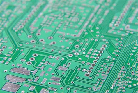
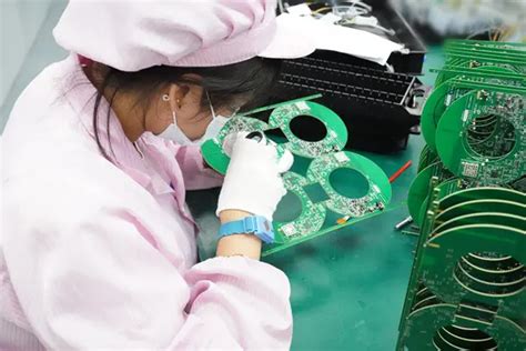
Printed Circuit Board (PCB) assembly is a meticulous process that requires precision and the right set of tools to ensure the highest quality and functionality of the final product. Among the various stages of PCB assembly, soldering is one of the most critical. Soldering involves joining electronic components to the PCB, and to achieve this with accuracy and reliability, several essential tools are indispensable.
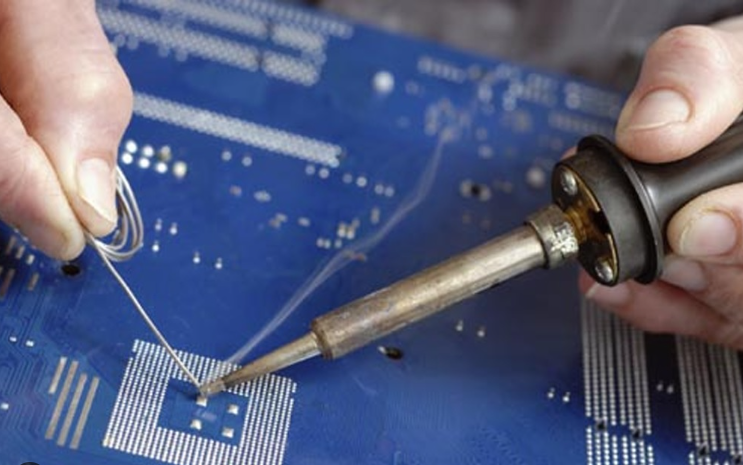
First and foremost, a high-quality soldering iron is fundamental.
This tool is used to heat the solder, allowing it to flow and create a secure connection between the component leads and the PCB pads. Modern soldering irons often come with adjustable temperature controls, which are crucial for working with different types of solder and components. A soldering station, which includes a soldering iron and a stand, often with integrated temperature control, is highly recommended for professional use.
In conjunction with the soldering iron, solder wire is another essential material.
Solder wire typically consists of a metal alloy, commonly a combination of tin and lead, although lead-free options are increasingly popular due to health and environmental concerns. The solder wire often contains a flux core, which helps to clean the surfaces being soldered and improve the flow of the solder. Flux is a chemical cleaning agent that removes oxidation from the metal surfaces, ensuring a strong bond.
To complement the soldering iron and solder wire, a desoldering tool is also necessary.
Desoldering tools, such as desoldering pumps or solder wick, are used to remove excess solder or to correct mistakes. A desoldering pump, also known as a solder sucker, is a mechanical device that creates a vacuum to suck up molten solder. Solder wick, on the other hand, is a braided copper wire that absorbs solder when heated. Both tools are invaluable for rework and repair tasks.
Precision is paramount in PCB assembly, and this is where tweezers come into play.
Tweezers are used to handle small components, especially surface-mount devices (SMDs), which can be challenging to manipulate with fingers alone. Anti-static tweezers are particularly important to prevent damage to sensitive electronic components from static electricity.
Another critical tool is the magnifying glass or microscope.
Given the miniature size of many electronic components and the fine pitch of PCB traces, visual inspection is essential to ensure proper solder joints and to identify any potential issues. Magnification tools allow for detailed examination, making it easier to spot defects such as solder bridges or cold joints.
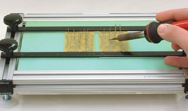
Additionally, a PCB holder or vise is highly beneficial.
This tool holds the PCB securely in place, allowing the assembler to work with both hands free. A stable work surface is crucial for precision and efficiency, reducing the risk of errors and improving overall workflow.
Lastly, safety equipment should not be overlooked.
Fume extractors are essential to remove harmful fumes generated during soldering, protecting the assembler’s health. Safety glasses and heat-resistant gloves can also provide additional protection against potential hazards.
In conclusion, the assembly of PCBs demands a range of specialized soldering tools to ensure precision, reliability, and safety. From soldering irons and desoldering tools to magnification devices and safety equipment, each tool plays a vital role in the successful assembly of electronic circuits. By investing in high-quality tools and understanding their proper use, one can achieve professional-grade results in PCB assembly.
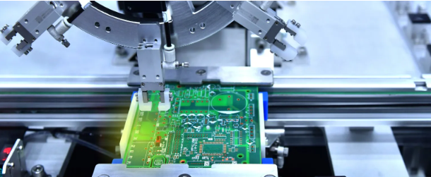
The Role Of Pick And Place Machines In PCB Assembly
In the realm of printed circuit board (PCB) assembly, the role of pick and place machines is indispensable. These sophisticated devices are designed to automate the placement of electronic components onto the PCB with remarkable precision and speed. As the demand for smaller, more complex electronic devices continues to grow, the importance of pick and place machines in the manufacturing process cannot be overstated.
To begin with, pick and place machines significantly enhance the efficiency of PCB assembly.
Traditionally, placing components onto a PCB was a manual process, requiring skilled technicians to meticulously position each part. This method was not only time-consuming but also prone to human error. In contrast, pick and place machines can handle thousands of components per hour, ensuring that each one is accurately placed according to the design specifications. This automation reduces the time required for assembly and minimizes the risk of errors, leading to higher productivity and lower production costs.
Moreover, the precision offered by pick and place machines is unparalleled.
These machines are equipped with advanced vision systems and robotic arms that can identify and place components with micron-level accuracy. This level of precision is crucial, especially for modern PCBs that feature densely packed components and intricate designs. The ability to place components accurately ensures that the final product functions as intended, which is vital for maintaining the quality and reliability of electronic devices.
In addition to efficiency and precision, pick and place machines also offer flexibility in the assembly process.
They can handle a wide variety of components, ranging from tiny surface-mount devices (SMDs) to larger through-hole components. This versatility allows manufacturers to use a single machine for different types of PCBs, reducing the need for multiple specialized machines and streamlining the production process. Furthermore, modern pick and place machines can be easily programmed and reconfigured to accommodate changes in design, making them ideal for both high-volume production and small-batch prototyping.
Another significant advantage of pick and place machines is their ability to integrate with other automated systems in the PCB assembly line.
For instance, they can work in conjunction with solder paste printers, reflow ovens, and automated optical inspection (AOI) systems to create a seamless and highly efficient production workflow. This integration not only speeds up the assembly process but also ensures that each step is performed with the highest level of accuracy and consistency.
Despite their numerous benefits, it is important to note that the successful implementation of pick and place machines requires careful planning and maintenance.
Manufacturers must ensure that the machines are properly calibrated and regularly serviced to maintain their performance. Additionally, operators need to be trained to handle the machines and troubleshoot any issues that may arise. By investing in proper training and maintenance, manufacturers can maximize the benefits of pick and place machines and ensure the smooth operation of their assembly lines.
In conclusion, pick and place machines play a crucial role in the PCB assembly process by enhancing efficiency, precision, and flexibility. Their ability to automate the placement of components not only speeds up production but also ensures the quality and reliability of the final product. As electronic devices continue to evolve and become more complex, the importance of these machines in the manufacturing process will only continue to grow. By integrating pick and place machines into their assembly lines, manufacturers can stay competitive in an increasingly demanding market and meet the ever-changing needs of their customers.
Importance Of Reflow Ovens In PCB Manufacturing
In the realm of printed circuit board (PCB) manufacturing, the importance of reflow ovens cannot be overstated. These sophisticated pieces of equipment play a pivotal role in ensuring the reliability and functionality of electronic devices. As the demand for smaller, more complex, and highly efficient electronic gadgets continues to surge, the precision and efficiency offered by reflow ovens become increasingly critical.
To begin with, reflow ovens are integral to the soldering process in PCB assembly.
They are designed to melt solder paste, which is applied to the PCB, thereby creating strong and reliable electrical connections between the components and the board. This process is essential for the functionality of the final product, as poor soldering can lead to weak connections, which may result in device failure. The reflow oven ensures that the solder paste is heated to the correct temperature, allowing it to flow and form a solid bond without damaging the components or the PCB itself.
Moreover, the precision of reflow ovens is a key factor in their importance.
These ovens are equipped with multiple heating zones, each of which can be precisely controlled to achieve the desired temperature profile. This level of control is crucial because different components on a PCB may have varying thermal requirements. For instance, some components may be sensitive to high temperatures and could be damaged if exposed to excessive heat. Reflow ovens allow manufacturers to tailor the heating process to accommodate these differences, ensuring that all components are soldered correctly without compromising their integrity.
In addition to precision, reflow ovens offer consistency, which is vital for large-scale PCB manufacturing.
The ability to replicate the same temperature profile across multiple boards ensures uniformity in the soldering process. This consistency is essential for maintaining the quality and reliability of the final products. Without it, manufacturers would face significant challenges in meeting industry standards and customer expectations. Reflow ovens, therefore, play a crucial role in streamlining the manufacturing process and enhancing productivity.
Furthermore, the use of reflow ovens contributes to the overall efficiency of PCB manufacturing.
Traditional soldering methods, such as hand soldering, are labor-intensive and time-consuming. In contrast, reflow ovens automate the soldering process, significantly reducing the time required to assemble PCBs. This automation not only speeds up production but also minimizes the risk of human error, which can lead to defects and rework. By improving efficiency and reducing the likelihood of errors, reflow ovens help manufacturers achieve higher yields and lower production costs.
Another important aspect to consider is the environmental impact of reflow ovens.
Modern reflow ovens are designed with energy efficiency in mind, utilizing advanced technologies to minimize energy consumption. This is particularly important in an era where sustainability is a growing concern. By reducing energy usage, reflow ovens contribute to the overall sustainability of the manufacturing process, aligning with the industry’s efforts to minimize its environmental footprint.
In conclusion, reflow ovens are indispensable tools in PCB manufacturing, offering precision, consistency, efficiency, and environmental benefits. Their ability to ensure reliable soldering connections, accommodate varying thermal requirements, and streamline the production process makes them a cornerstone of modern electronics manufacturing. As technology continues to evolve, the role of reflow ovens in producing high-quality, reliable electronic devices will only become more significant.
Advanced Inspection Tools For PCB Quality Control
In the realm of printed circuit board (PCB) assembly, ensuring the highest quality of the final product is paramount. Advanced inspection tools play a crucial role in maintaining this quality, as they allow for the detection and rectification of defects that could compromise the functionality and reliability of the PCB. These tools have evolved significantly over the years, incorporating cutting-edge technologies to provide more accurate and efficient inspection processes.
One of the most widely used advanced inspection tools in PCB quality control is Automated Optical Inspection (AOI).
AOI systems utilize high-resolution cameras and sophisticated algorithms to capture and analyze images of the PCB. By comparing these images to a predefined set of standards, AOI systems can identify a wide range of defects, including misaligned components, soldering issues, and missing parts. The speed and precision of AOI make it an indispensable tool in modern PCB manufacturing, as it allows for rapid detection and correction of errors, thereby reducing the likelihood of defective products reaching the end user.
In addition to AOI, X-ray inspection systems have become increasingly important in PCB quality control.
These systems are particularly useful for inspecting multi-layer PCBs and components with hidden solder joints, such as Ball Grid Arrays (BGAs). X-ray inspection provides a non-destructive means of examining the internal structure of the PCB, enabling the detection of defects that are not visible to the naked eye or through optical inspection. This capability is essential for ensuring the integrity of complex PCBs, where even minor defects can lead to significant performance issues.
Another advanced inspection tool that has gained prominence in recent years is Automated X-ray Inspection (AXI).
AXI combines the principles of X-ray inspection with automation, allowing for the rapid and thorough examination of PCBs. By automating the inspection process, AXI systems can handle large volumes of PCBs with consistent accuracy, making them ideal for high-volume manufacturing environments. The ability to detect and analyze defects in real-time further enhances the efficiency of the quality control process, as it enables immediate corrective actions to be taken.
Furthermore, the integration of machine learning and artificial intelligence (AI) into inspection tools has revolutionized PCB quality control.
These technologies enable inspection systems to learn from previous inspections and improve their accuracy over time. For instance, AI-powered AOI systems can adapt to variations in component placement and soldering, reducing the likelihood of false positives and negatives. This adaptability is particularly valuable in the context of modern PCB manufacturing, where the complexity and variability of designs continue to increase.
Moreover, the use of 3D inspection tools has also become more prevalent in PCB quality control. Unlike traditional 2D inspection methods, 3D inspection provides a more comprehensive view of the PCB, allowing for the detection of defects related to component height, coplanarity, and solder volume. This additional dimension of inspection is crucial for ensuring the reliability of advanced PCBs, which often feature densely packed components and intricate designs.
In conclusion, advanced inspection tools are indispensable for maintaining the quality and reliability of PCBs. The integration of technologies such as AOI, X-ray inspection, AXI, machine learning, and 3D inspection has significantly enhanced the accuracy and efficiency of the inspection process. As PCB designs continue to evolve and become more complex, the importance of these advanced inspection tools will only grow, ensuring that manufacturers can consistently deliver high-quality products to their customers.