Pcb board design
Best Practices For Pcb board design
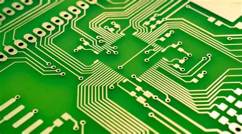
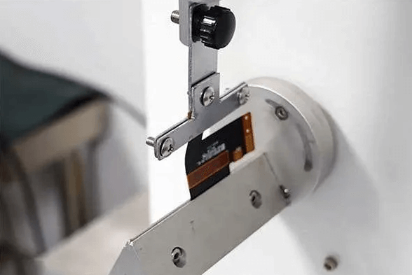
Printed Circuit Board (PCB) layout design is a critical aspect of electronics engineering, requiring meticulous attention to detail and adherence to best practices to ensure optimal performance and reliability.
One of the fundamental principles in PCB layout design is the strategic placement of components.
Proper component placement not only facilitates efficient signal routing but also minimizes potential interference and noise. It is advisable to place components with similar functions together and to keep high-speed signal paths as short as possible to reduce signal degradation.
Transitioning to another crucial aspect, the importance of grounding cannot be overstated.
A well-designed ground plane is essential for maintaining signal integrity and reducing electromagnetic interference (EMI). Ensuring a continuous ground plane beneath signal traces can significantly enhance the performance of the PCB. Additionally, it is beneficial to use multiple ground vias to connect different layers of the PCB, thereby providing a low-impedance path for return currents.
Another best practice involves the careful routing of signal traces.
Signal integrity is paramount, and to achieve this, designers should avoid sharp angles in trace routing, opting instead for smooth, curved paths. This reduces the risk of signal reflection and impedance discontinuities. Furthermore, maintaining consistent trace widths and spacing is vital to prevent crosstalk and ensure uniform impedance. Differential pairs, commonly used for high-speed signals, should be routed together with equal lengths to maintain signal timing and integrity.
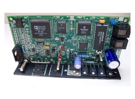
Thermal management is another critical consideration in PCB layout design.
Components that generate significant heat, such as power transistors and voltage regulators, should be placed in areas with adequate ventilation and, if necessary, supplemented with heat sinks or thermal vias. Proper thermal management not only extends the lifespan of the components but also ensures the overall reliability of the PCB.
In addition to thermal considerations, power distribution is a key factor in PCB design.
Ensuring that power traces are sufficiently wide to handle the required current without excessive voltage drop is essential. Utilizing power planes can help distribute power more evenly and reduce the complexity of routing. Decoupling capacitors should be placed as close as possible to the power pins of integrated circuits to filter out noise and provide a stable power supply.
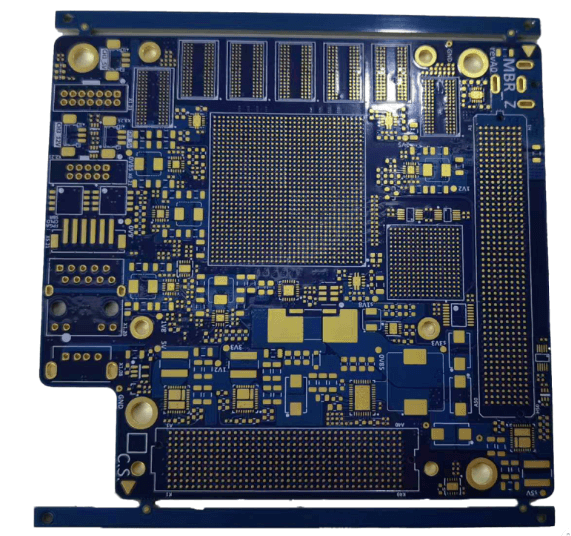
Design for manufacturability (DFM) is another best practice that should be integrated into the PCB layout process.
This involves considering the limitations and capabilities of the manufacturing process to ensure that the PCB can be produced reliably and cost-effectively. For instance, maintaining adequate spacing between traces and pads, avoiding the use of excessively small vias, and ensuring that all components are accessible for soldering and inspection are all critical DFM considerations.
Lastly, thorough design rule checks (DRC) and electrical rule checks (ERC) are indispensable in the PCB layout design process.
These automated checks help identify potential issues such as spacing violations, unconnected nets, and other design errors that could compromise the functionality of the PCB. By rigorously adhering to these best practices, designers can create PCB layouts that are not only functional and efficient but also robust and reliable, ensuring the successful operation of the final electronic product.
Common Mistakes To Avoid In PCB Design
Printed Circuit Board (PCB) design is a critical aspect of modern electronics, serving as the backbone for virtually all electronic devices. However, even experienced designers can fall prey to common mistakes that can compromise the functionality, reliability, and manufacturability of a PCB. Understanding these pitfalls and how to avoid them is essential for producing high-quality boards.
One frequent mistake in PCB design is inadequate planning of the board layout.
Designers often rush into the placement of components without considering the overall architecture of the board. This can lead to inefficient use of space and problematic routing of traces. To avoid this, it is crucial to start with a well-thought-out plan that considers the placement of all major components and the flow of signals between them. This initial step can save significant time and effort in the later stages of design.
Another common error is the improper management of signal integrity.
High-speed signals are particularly susceptible to issues such as crosstalk, reflection, and electromagnetic interference (EMI). To mitigate these problems, designers should pay close attention to trace impedance, routing techniques, and the use of ground planes. For instance, maintaining consistent trace widths and avoiding sharp angles can help preserve signal integrity. Additionally, placing ground planes adjacent to signal layers can provide a return path for high-frequency currents, thereby reducing EMI.
Thermal management is another critical aspect that is often overlooked.
Components that generate significant heat can affect the performance and longevity of the PCB if not properly managed. Designers should ensure adequate thermal vias, heat sinks, and copper pours to dissipate heat effectively. Failing to address thermal issues can lead to overheating, which may cause components to fail or degrade over time.
Furthermore, designers frequently make the mistake of not adhering to design for manufacturability (DFM) guidelines.
These guidelines are essential for ensuring that the PCB can be produced reliably and cost-effectively. Ignoring DFM considerations can result in boards that are difficult or impossible to manufacture, leading to increased costs and delays. To avoid this, designers should collaborate closely with manufacturers during the design process and adhere to their specific requirements and capabilities.
Another area where mistakes are common is in the selection and placement of decoupling capacitors.
These capacitors are crucial for stabilizing power supply voltages and filtering out noise. However, placing them too far from the components they are meant to support can render them ineffective. Designers should place decoupling capacitors as close as possible to the power pins of integrated circuits to ensure optimal performance.
Additionally, neglecting to perform thorough design rule checks (DRCs) and electrical rule checks (ERCs) can lead to significant issues.
These automated checks can identify potential problems such as short circuits, spacing violations, and incorrect net connections. Regularly running DRCs and ERCs throughout the design process can help catch errors early, reducing the risk of costly revisions later.
Lastly, documentation is an often-overlooked aspect of PCB design.
Comprehensive documentation, including schematics, layout files, and bill of materials (BOM), is essential for successful manufacturing and assembly. Incomplete or inaccurate documentation can lead to misunderstandings and errors during production. Ensuring that all documentation is thorough and up-to-date can facilitate a smoother transition from design to manufacturing.
In conclusion, avoiding common mistakes in PCB design requires careful planning, attention to detail, and adherence to best practices. By addressing issues related to layout, signal integrity, thermal management, manufacturability, decoupling capacitor placement, rule checks, and documentation, designers can create reliable and efficient PCBs that meet the demands of modern electronic applications.
Advanced Techniques For High-Speed PCB Design
In the realm of high-speed PCB design, advanced techniques are essential to ensure optimal performance and reliability. As electronic devices continue to evolve, the demand for faster processing speeds and higher data rates has necessitated the development of sophisticated design methodologies. One of the primary considerations in high-speed PCB design is signal integrity, which refers to the preservation of signal quality as it travels through the circuit. To achieve this, designers must meticulously manage impedance, minimize crosstalk, and control electromagnetic interference (EMI).
Impedance control is a critical aspect of high-speed PCB design.
It involves maintaining a consistent impedance along the signal paths to prevent signal reflections, which can cause data corruption. This is typically achieved by carefully selecting the trace width, spacing, and the dielectric material of the PCB. Additionally, the use of differential pairs, where two complementary signals are routed together, can help maintain signal integrity by reducing susceptibility to external noise and crosstalk.
Crosstalk, the unwanted coupling of signals between adjacent traces, can significantly degrade the performance of high-speed circuits.
To mitigate crosstalk, designers often employ techniques such as increasing the spacing between traces, using ground planes to provide a return path for signals, and implementing guard traces. Guard traces are grounded traces placed between signal lines to shield them from interference. Furthermore, proper layer stack-up design, where signal layers are sandwiched between ground and power planes, can also help reduce crosstalk and improve overall signal integrity.
Electromagnetic interference (EMI) is another challenge in high-speed PCB design.
EMI can originate from various sources, including switching power supplies, clock signals, and high-speed data lines. To minimize EMI, designers can use techniques such as shielding, filtering, and careful layout planning. Shielding involves enclosing sensitive components or entire circuits in a conductive enclosure to block external electromagnetic fields. Filtering can be achieved by incorporating components like ferrite beads, capacitors, and inductors to suppress high-frequency noise. Additionally, maintaining short and direct signal paths, avoiding sharp corners in trace routing, and using proper grounding techniques can further reduce EMI.
Power integrity is equally important in high-speed PCB design.
Ensuring a stable and clean power supply to all components is crucial for maintaining signal integrity and overall system performance. Designers must pay attention to power distribution networks (PDNs), which include power planes, decoupling capacitors, and vias. Proper placement and selection of decoupling capacitors can help filter out noise and provide a stable power supply. Moreover, using multiple power and ground planes can reduce impedance and improve current distribution.
Thermal management is another vital consideration in high-speed PCB design.
As components operate at higher speeds, they tend to generate more heat, which can affect performance and reliability. Effective thermal management techniques include using thermal vias to transfer heat from hot components to other layers, incorporating heat sinks, and designing PCBs with adequate airflow. Additionally, selecting materials with high thermal conductivity and optimizing the layout to distribute heat evenly can help manage thermal challenges.
In conclusion, advanced techniques for high-speed PCB design are essential to meet the demands of modern electronic devices. By focusing on signal integrity, crosstalk reduction, EMI control, power integrity, and thermal management, designers can create PCBs that perform reliably at high speeds. As technology continues to advance, the importance of these techniques will only grow, making them indispensable tools for engineers in the field of PCB design.
The Role Of Thermal Management In PCB Design
In the realm of printed circuit board (PCB) design, thermal management plays a pivotal role in ensuring the reliability and longevity of electronic devices. As electronic components become increasingly powerful and compact, the heat they generate can pose significant challenges. Effective thermal management is essential to mitigate these challenges and maintain optimal performance.
To begin with, it is important to understand the sources of heat within a PCB.
Components such as processors, power transistors, and integrated circuits are primary contributors to heat generation. When these components operate, they convert electrical energy into heat, which must be dissipated to prevent overheating. Overheating can lead to component failure, reduced efficiency, and even catastrophic damage to the entire system.
One of the fundamental strategies in thermal management is the use of thermal vias.
These are small holes filled with conductive material, typically copper, that facilitate the transfer of heat from the surface of the PCB to the inner layers or to an external heat sink. By providing a pathway for heat to escape, thermal vias help in maintaining a lower temperature for critical components. Additionally, the placement and number of thermal vias must be carefully considered during the design phase to ensure effective heat dissipation without compromising the structural integrity of the PCB.
Another crucial aspect of thermal management is the selection of appropriate materials.
The thermal conductivity of the substrate material can significantly influence the overall thermal performance of the PCB. Materials such as FR-4, a common PCB substrate, have relatively low thermal conductivity. In contrast, materials like metal-core PCBs (MCPCBs) offer higher thermal conductivity and are often used in high-power applications. The choice of material should align with the thermal requirements of the specific application to ensure efficient heat dissipation.
Moreover, the layout of components on the PCB can greatly impact thermal management.
Components that generate significant heat should be strategically placed to avoid hotspots and ensure even heat distribution. For instance, high-power components should be positioned away from temperature-sensitive components to prevent thermal interference. Additionally, the use of thermal relief pads can aid in managing heat by providing a controlled path for heat to flow away from critical areas.
Heat sinks and thermal interface materials (TIMs) are also integral to effective thermal management.
Heat sinks, typically made of aluminum or copper, are attached to heat-generating components to increase the surface area for heat dissipation. TIMs, such as thermal grease or thermal pads, are used to fill the microscopic gaps between the heat sink and the component, enhancing thermal conductivity. The combination of heat sinks and TIMs ensures efficient heat transfer from the component to the surrounding environment.
Furthermore, thermal simulation and analysis tools are invaluable in the PCB design process.
These tools allow designers to model and predict the thermal behavior of the PCB under various operating conditions. By simulating different scenarios, designers can identify potential thermal issues and make informed decisions to optimize the thermal performance of the PCB. This proactive approach helps in minimizing the risk of thermal-related failures and enhances the overall reliability of the electronic device.
In conclusion, thermal management is a critical consideration in PCB design that directly impacts the performance and durability of electronic devices. Through the strategic use of thermal vias, appropriate material selection, thoughtful component layout, and the incorporation of heat sinks and TIMs, designers can effectively manage heat dissipation. Additionally, leveraging thermal simulation tools enables designers to anticipate and address thermal challenges, ensuring the successful operation of the PCB in real-world applications. As electronic devices continue to evolve, the importance of robust thermal management in PCB design cannot be overstated.