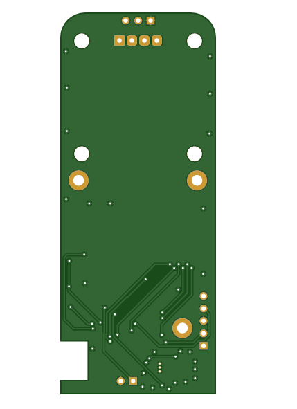
Pcb board layout
Best Practices For PCB Layout Design
Designing a printed circuit board (PCB) is a critical step in the development of electronic devices, requiring meticulous attention to detail and adherence to best practices to ensure functionality, reliability, and manufacturability.
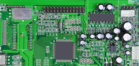
One of the foremost considerations in PCB layout design is the placement of components.
Proper component placement is essential for optimizing signal flow, minimizing interference, and ensuring thermal management. Components should be arranged logically, with related components placed in proximity to each other to reduce the length of signal paths. This not only enhances performance but also simplifies troubleshooting and testing.
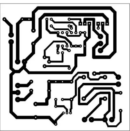
Transitioning from component placement, another crucial aspect is the routing of traces.
Effective trace routing involves creating paths for electrical signals to travel between components. It is imperative to keep traces as short and direct as possible to minimize resistance and inductance, which can degrade signal integrity. Additionally, designers should avoid sharp angles in trace routing, as these can cause signal reflections and potential points of failure. Instead, using smooth, curved traces or 45-degree angles can help maintain signal quality.
Furthermore, the importance of grounding cannot be overstated in PCB layout design.
A well-designed ground plane provides a common reference point for all components and helps to reduce electromagnetic interference (EMI). Ensuring a continuous ground plane with minimal interruptions is vital for maintaining signal integrity and reducing noise. Designers should also consider the placement of decoupling capacitors near power pins of integrated circuits to filter out noise and stabilize the power supply.
Thermal management is another critical factor in PCB layout design.
As electronic components generate heat during operation, it is essential to manage this heat effectively to prevent damage and ensure longevity. Designers should strategically place heat-generating components and provide adequate spacing to allow for proper airflow. Additionally, incorporating thermal vias and heat sinks can help dissipate heat more efficiently. It is also advisable to use thermal relief pads for through-hole components to facilitate soldering and improve thermal performance.
Transitioning to the topic of design rules, adhering to design for manufacturability (DFM) guidelines is paramount.
DFM guidelines ensure that the PCB can be manufactured reliably and cost-effectively. This includes considerations such as minimum trace width and spacing, hole sizes, and solder mask clearance. By following these guidelines, designers can avoid common manufacturing issues such as short circuits, open circuits, and solder bridging.
Moreover, signal integrity is a key consideration in high-speed PCB designs.
To maintain signal integrity, designers should pay attention to impedance control, crosstalk, and signal reflection. Controlled impedance traces, differential pairs, and proper termination techniques can help mitigate these issues. Additionally, separating high-speed signals from noisy power and ground planes can further enhance signal integrity.
In conclusion, best practices for PCB layout design encompass a range of considerations, from component placement and trace routing to grounding, thermal management, and adherence to DFM guidelines. By meticulously addressing each of these aspects, designers can create PCBs that are not only functional and reliable but also manufacturable and cost-effective. Employing these best practices ensures that the final product meets performance requirements and stands the test of time in real-world applications.
Common Mistakes In PCB Layout And How To Avoid Them
Printed Circuit Board (PCB) layout is a critical aspect of electronic design, serving as the foundation upon which the functionality and reliability of electronic devices are built. However, even experienced designers can fall prey to common mistakes that can compromise the performance and manufacturability of a PCB. Understanding these pitfalls and learning how to avoid them is essential for creating robust and efficient designs.
One prevalent mistake in PCB layout is inadequate component placement.
Poorly placed components can lead to a host of issues, including signal integrity problems, increased electromagnetic interference (EMI), and difficulty in routing traces. To avoid this, designers should prioritize placing components with high pin counts or those that are critical to the circuit’s functionality first. Additionally, grouping related components together and maintaining a logical flow can significantly enhance the layout’s efficiency.
Another frequent error is improper trace routing.
Traces that are too long, too narrow, or routed at sharp angles can introduce resistance, inductance, and potential signal reflections, all of which can degrade the circuit’s performance. To mitigate these issues, designers should aim to keep traces as short and direct as possible, use appropriate trace widths based on current-carrying requirements, and avoid acute angles by using 45-degree bends instead of 90-degree turns.
Grounding issues also commonly plague PCB layouts.
A poor grounding strategy can result in ground loops, increased noise, and potential circuit instability. To ensure a solid grounding scheme, designers should use a ground plane whenever possible, which provides a low-impedance path for return currents and helps to minimize EMI. Additionally, connecting all ground points to a single ground plane can prevent ground loops and ensure a stable reference voltage throughout the circuit.
Thermal management is another critical aspect that is often overlooked.
Components that generate significant heat can affect the performance and longevity of the PCB if not properly managed. To address this, designers should place heat-generating components in areas with good airflow and use thermal vias to dissipate heat through the PCB layers. Additionally, incorporating heat sinks or thermal pads can further aid in managing excessive heat.
Design rule violations are another common pitfall.
Failing to adhere to the design rules specified by the PCB manufacturer can result in boards that are difficult or impossible to fabricate. To avoid this, designers should familiarize themselves with the manufacturer’s capabilities and constraints, such as minimum trace widths, spacing, and hole sizes. Utilizing design rule checks (DRC) within the PCB design software can help identify and rectify violations before the board goes into production.
Signal integrity issues, such as crosstalk and impedance mismatches, can also arise from poor PCB layout practices.
To mitigate these problems, designers should maintain adequate spacing between high-speed signal traces and use controlled impedance routing techniques. Additionally, incorporating proper termination methods and using differential pairs for high-speed signals can further enhance signal integrity.
In conclusion, avoiding common mistakes in PCB layout requires a combination of careful planning, adherence to best practices, and thorough verification. By prioritizing proper component placement, optimizing trace routing, ensuring robust grounding, managing thermal considerations, adhering to design rules, and addressing signal integrity concerns, designers can create reliable and high-performance PCBs. Through continuous learning and attention to detail, the likelihood of encountering these pitfalls can be significantly reduced, leading to more successful electronic designs.
Advanced Techniques For High-Speed PCB Layout
In the realm of high-speed PCB (Printed Circuit Board) design, advanced techniques are essential to ensure optimal performance and reliability. As electronic devices become increasingly sophisticated, the demand for faster data transmission rates and higher processing speeds necessitates meticulous attention to PCB layout. One of the primary considerations in high-speed PCB design is signal integrity, which can be significantly affected by factors such as impedance control, crosstalk, and electromagnetic interference (EMI).
To begin with, impedance control is crucial in high-speed PCB layouts.
Impedance mismatches can lead to signal reflections, which degrade signal quality and can cause data errors. To mitigate this, designers must carefully calculate and maintain the characteristic impedance of transmission lines. This involves selecting appropriate trace widths, spacing, and dielectric materials. Utilizing tools such as impedance calculators and simulation software can aid in achieving precise impedance control, thereby enhancing signal integrity.
In addition to impedance control, managing crosstalk is vital in high-speed PCB design.
Crosstalk occurs when a signal in one trace induces unwanted noise in an adjacent trace, potentially leading to data corruption. To minimize crosstalk, designers should maintain adequate spacing between high-speed traces and employ differential signaling where possible. Differential pairs, which consist of two complementary signals, can effectively cancel out noise and reduce susceptibility to crosstalk. Furthermore, incorporating ground planes and shielding techniques can provide additional isolation and protection against crosstalk.
Electromagnetic interference (EMI) is another critical concern in high-speed PCB layouts.
EMI can emanate from various sources, including power supplies, clock signals, and high-speed data lines. To combat EMI, designers should implement proper grounding and decoupling strategies. A solid ground plane can serve as a reference point for signals and help dissipate unwanted noise. Additionally, placing decoupling capacitors close to power pins can filter out high-frequency noise and stabilize power delivery. Employing ferrite beads and EMI shields can further attenuate electromagnetic emissions and enhance overall PCB performance.
Transitioning to the topic of signal routing, it is imperative to follow best practices to ensure signal integrity and minimize potential issues.
High-speed signals should be routed with minimal layer transitions to avoid introducing impedance discontinuities. When layer changes are necessary, using vias with controlled impedance can help maintain signal integrity. Additionally, designers should avoid sharp corners in trace routing, as these can cause signal reflections and degrade performance. Instead, using smooth, gradual bends can help maintain consistent impedance and reduce signal degradation.
Another advanced technique in high-speed PCB layout is the use of controlled impedance stack-ups.
A well-designed stack-up can provide a balanced distribution of signal layers and reference planes, which is essential for maintaining signal integrity. By carefully selecting the order and thickness of each layer, designers can achieve the desired impedance characteristics and minimize signal loss. Simulation tools can be invaluable in optimizing stack-up configurations and ensuring that the final design meets performance requirements.
Finally, thermal management is a critical aspect of high-speed PCB design.
As components operate at higher speeds, they generate more heat, which can affect performance and reliability. Effective thermal management techniques, such as using thermal vias, heat sinks, and proper component placement, can help dissipate heat and maintain optimal operating temperatures. Additionally, thermal simulation tools can assist in identifying potential hotspots and optimizing the thermal performance of the PCB.
In conclusion, advanced techniques for high-speed PCB layout are essential for achieving optimal performance and reliability in modern electronic devices. By focusing on impedance control, crosstalk management, EMI mitigation, signal routing best practices, controlled impedance stack-ups, and thermal management, designers can create high-speed PCBs that meet the demanding requirements of today’s technology. Employing these techniques and leveraging simulation tools can significantly enhance the design process and ensure the successful implementation of high-speed electronic systems.
The Importance Of Grounding In PCB Layout
In the realm of printed circuit board (PCB) design, grounding is a fundamental aspect that significantly influences the performance, reliability, and safety of electronic devices. Grounding, in essence, refers to the method of creating a common return path for electric current, which is crucial for maintaining the integrity of the electrical signals and ensuring the proper functioning of the circuit. The importance of grounding in PCB layout cannot be overstated, as it plays a pivotal role in mitigating noise, reducing electromagnetic interference (EMI), and preventing potential damage to components.
To begin with, grounding is essential for noise reduction in PCB layouts.
Electrical noise, which can arise from various sources such as power supply fluctuations, switching transients, and external electromagnetic fields, can severely affect the performance of a circuit. By establishing a solid grounding scheme, designers can create a low-impedance path for the return currents, thereby minimizing the potential for noise to interfere with the signal integrity. This is particularly critical in high-speed digital circuits, where even minor noise can lead to data corruption and signal degradation.
Moreover, grounding is instrumental in reducing electromagnetic interference.
EMI is a common issue in electronic systems, where unwanted electromagnetic waves can disrupt the normal operation of the circuit. A well-designed grounding system helps to shield sensitive components from these disturbances by providing a reference point for the electric fields. This is achieved through the use of ground planes, which are large areas of copper on the PCB that serve as a common ground reference. Ground planes not only help in reducing EMI but also improve the overall thermal management of the PCB by dissipating heat more effectively.
In addition to noise reduction and EMI mitigation, grounding is crucial for the safety and reliability of electronic devices.
Proper grounding ensures that any fault currents, which may occur due to component failures or external surges, are safely directed away from sensitive components and towards the ground. This helps in preventing potential damage to the circuit and reduces the risk of electric shock to users. Furthermore, grounding provides a stable reference voltage for the entire circuit, which is essential for the accurate operation of analog and digital components.
Transitioning to the practical aspects of grounding in PCB layout, designers must consider several key factors to achieve an effective grounding scheme.
One of the primary considerations is the placement of ground vias, which are vertical connections that link different layers of the PCB. Strategically placing ground vias near high-frequency components and along the return current paths can significantly enhance the grounding effectiveness. Additionally, designers should aim to minimize the length of ground traces, as longer traces can introduce inductance and resistance, which can degrade the grounding performance.
Another important aspect is the separation of analog and digital grounds.
In mixed-signal circuits, where both analog and digital components coexist, it is crucial to isolate the grounds to prevent digital noise from contaminating the analog signals. This can be achieved by creating separate ground planes for analog and digital sections and connecting them at a single point, often referred to as a star ground.
In conclusion, grounding is a critical element in PCB layout that impacts the noise performance, EMI resilience, and overall safety of electronic devices. By understanding and implementing effective grounding techniques, designers can ensure the optimal functioning and reliability of their circuits. As electronic systems continue to evolve and become more complex, the importance of grounding in PCB design will only continue to grow, underscoring the need for meticulous attention to this fundamental aspect.


.png)