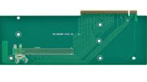
PCB Card Edge Connector Area: Design Considerations and Optimization
Introduction
Printed Circuit Board (PCB) card edge connectors represent a critical interface technology in modern electronics, providing a direct, cost-effective connection between PCBs without requiring additional connector components. The design of the PCB area dedicated to these connectors—commonly referred to as the “card edge interface area”—significantly impacts the reliability, signal integrity, and mechanical stability of the entire system. This article explores the key considerations for designing and optimizing the PCB card edge connector area, covering electrical, mechanical, and manufacturing aspects that engineers must address to ensure robust performance.
Fundamentals of PCB Card Edge Connectors
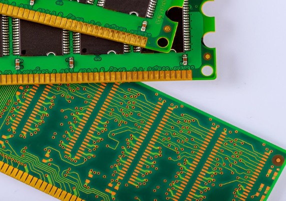
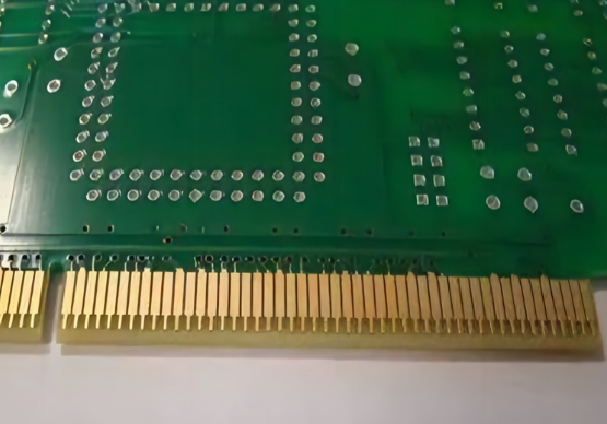
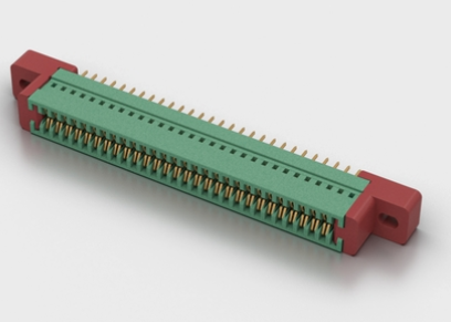
PCB card edge connectors utilize exposed copper traces along the edge of a PCB that mate with corresponding spring-loaded contacts in a receptacle connector. This interface area must be carefully designed to meet several simultaneous requirements:
- Electrical Contact Reliability: The exposed copper must maintain good conductivity through multiple insertion cycles
- Mechanical Durability: The edge must withstand physical wear from repeated connections
- Signal Integrity: The interface must maintain proper impedance and minimize signal degradation
- Manufacturing Precision: The edge must be fabricated to tight tolerances for proper mating
The typical card edge connector area consists of several key features:
- Contact fingers (exposed copper pads)
- Guide notches or keying features
- Beveled edge for easier insertion
- Plating (often gold over nickel) on contact surfaces
- Appropriate solder mask and silkscreen exclusion zones
Electrical Design Considerations
Contact Pad Layout and Spacing
The arrangement of contact pads in the card edge area follows several industry standards depending on application:
- PCI Express: 0.8mm or 1.0mm pitch
- PCI: 1.27mm pitch
- Custom Designs: Variable pitch as needed
Key electrical parameters for contact pads:
- Pad Width: Typically 0.4-0.6mm for 1.27mm pitch designs
- Pad Length: 3-5mm is common for adequate contact wipe
- Spacing: Maintains electrical isolation and affects impedance
Impedance Control
Maintaining consistent impedance through the connector area prevents signal reflections:
- Microstrip Configuration: Most common for surface traces
- Requires careful control of dielectric thickness
- Affected by solder mask presence/absence
- Stripline Configuration: For internal layers transitioning to edge
- Requires symmetrical construction
- More challenging to control at board edge
Impedance discontinuities should be minimized through:
- Gradual trace width transitions
- Minimizing layer changes near the edge
- Proper termination of unused reference planes
Power Delivery
High-current applications require special consideration:
- Multiple adjacent contacts for each power rail
- Wider power contacts when possible
- Proper plane connections behind contacts
- Possible use of buried vias near edge
Mechanical Design Factors
Board Edge Preparation
The physical edge of the PCB requires precise machining:
- Bevel Angle: Typically 30°-45° for easier insertion
- Edge Roughness: <50μm recommended for smooth mating
- Dimensional Tolerance: ±0.1mm critical for reliable contact
Contact Finger Plating
Common plating options for the contact area:
- Hard Gold (0.5-1.27μm over 2.5-5μm nickel):
- Excellent wear resistance
- 1000+ insertion cycles
- Higher cost
- Soft Gold (1-2.5μm over nickel):
- Better conductivity
- Limited to ~100 insertions
- Lower cost
- Selective Gold (gold only on contact areas):
- Cost optimization
- Requires precise masking
Keying and Polarization
Prevents incorrect insertion through:
- Asymmetrical notch placement
- Varied contact patterns
- Physical blockers for reverse insertion
Mechanical Reinforcement
High-insertion-cycle applications may require:
- Increased board thickness near edge
- Additional stiffeners
- Strategic placement of mounting holes
Manufacturing Considerations
PCB Fabrication Tolerances
Critical dimensions requiring tight control:
- Contact finger width and spacing (±0.05mm)
- Edge straightness (<0.1mm over length)
- Plating thickness uniformity (±10%)
Solder Mask and Silkscreen
Proper application around the edge connector:
- Clearance from contact fingers (typically 0.2-0.5mm)
- Avoidance of mask over contacts
- Possible use of peelable mask for plating protection
Beveling Process
Edge preparation methods:
- Router Beveling: Most common, cost-effective
- Grinding: For higher precision requirements
- Laser Cutting: For very fine pitch designs
Reliability and Testing
Insertion Force Analysis
Factors affecting mating force:
- Contact normal force (typically 50-150g per contact)
- Number of contacts
- Bevel angle and smoothness
- Connector design
Wear Testing
Evaluation methods:
- Insertion/extraction cycling
- Contact resistance monitoring
- Visual inspection of wear patterns
Environmental Testing
Should include:
- Temperature cycling
- Humidity exposure
- Corrosion resistance
- Vibration testing
Advanced Design Techniques
High-Speed Optimization
For signals above 1GHz:
- Ground contacts interspersed with signals
- Matched length contacts for differential pairs
- Possible use of edge-coupled designs
High-Density Designs
Approaches for miniaturization:
- Fine pitch contacts (0.5mm or less)
- Two-sided edge contacts
- Staggered contact arrangements
Mixed-Signal Designs
Strategies for noise reduction:
- Careful separation of analog and digital contacts
- Guard contacts between sensitive signals
- Proper grounding schemes
Industry Standards
Relevant standards for card edge connectors:
- IEC 60603: General requirements
- PCI Express Card Electromechanical Spec
- VMEbus specifications
- Custom standards for proprietary implementations
Conclusion
The PCB card edge connector area represents a complex interface requiring careful balance of electrical, mechanical, and manufacturing considerations. Successful designs must account for signal integrity requirements, mechanical durability needs, and production capabilities while meeting cost targets. As electronic systems continue to demand higher speeds and greater reliability, the importance of proper card edge connector area design only grows more critical. By applying the principles discussed in this article and staying current with evolving connector technologies, engineers can develop robust, high-performance edge connector implementations suitable for their specific application requirements.
Future trends in card edge connector technology may include:
- Even finer pitch designs for increased density
- Advanced plating materials for extended durability
- Integrated shielding techniques for improved EMI performance
- Active alignment features for high-precision applications
The card edge connector remains a vital interconnection technology, and its proper implementation on PCBs will continue to be essential for electronic system performance and reliability.