PCB Catastrophic Failures: Causes, Consequences, and Prevention
Introduction
Printed Circuit Boards (PCBs) are the backbone of modern electronics, found in everything from consumer gadgets to industrial machinery and aerospace systems. While PCBs are designed for reliability, catastrophic failures can occur due to various factors, leading to system malfunctions, safety hazards, and financial losses. This article explores the root causes of PCB catastrophic failures, their consequences, and strategies for prevention.
1. Understanding Catastrophic PCB Failures
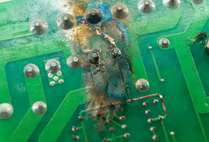
A catastrophic failure refers to a sudden and irreversible malfunction that renders a PCB completely non-functional. Unlike gradual degradation, catastrophic failures often occur without warning and can result in:
- Complete loss of functionality
- Fire or explosion risks
- Damage to connected components
- Safety hazards in critical applications (e.g., medical devices, automotive systems)

2. Common Causes of Catastrophic PCB Failures
2.1 Electrical Overstress (EOS) and Electrostatic Discharge (ESD)
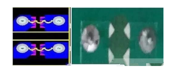
- EOS occurs when a PCB is subjected to excessive voltage or current beyond its design limits, leading to burnt traces, blown components, or dielectric breakdown.
- ESD can instantly damage sensitive semiconductor components, causing latent or immediate failure.
2.2 Thermal Overload and Thermal Cycling
- Overheating due to poor thermal management can melt solder joints, delaminate layers, or cause component failure.
- Thermal cycling (repeated heating and cooling) induces mechanical stress, leading to cracked traces or solder fatigue.
2.3 Mechanical Stress and Physical Damage
- Vibration and shock (e.g., in automotive or aerospace applications) can fracture solder joints or break components.
- Flexing or bending of rigid PCBs can crack internal traces or cause short circuits.
2.4 Manufacturing Defects
- Poor soldering (cold joints, voids, or bridging) can lead to intermittent or complete failure.
- Contamination (flux residues, moisture, or metallic debris) can cause corrosion or short circuits.
- Layer misalignment in multilayer PCBs can result in impedance mismatches or open circuits.
2.5 Environmental Factors
- Moisture ingress can lead to corrosion, dendritic growth, and electrochemical migration.
- Chemical exposure (e.g., in industrial environments) can degrade PCB materials over time.
2.6 Design Flaws
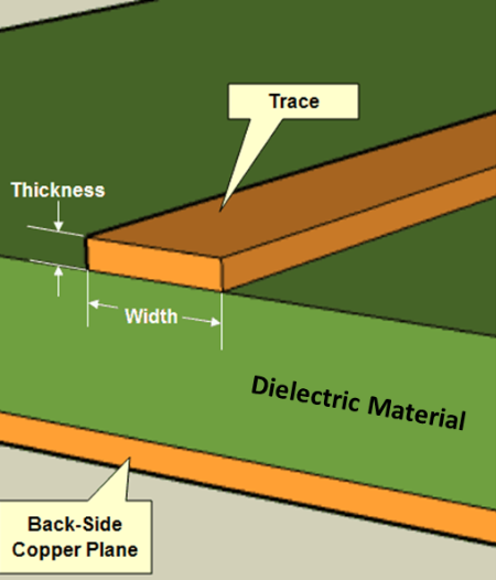
- Insufficient trace width for high-current paths can cause overheating.
- Poor grounding and EMI shielding may lead to signal integrity issues or latch-up events.
- Inadequate spacing between high-voltage traces can result in arcing.
3. Consequences of Catastrophic PCB Failures
The impact of PCB failures varies depending on the application:
3.1 Consumer Electronics
- Device malfunction, data loss, or safety risks (e.g., battery fires in smartphones).
3.2 Automotive and Aerospace Systems
- Sudden system failure in critical components (e.g., engine control units, avionics) can lead to accidents.
3.3 Medical Devices
- Life-support equipment failures can have fatal consequences.
3.4 Industrial and Power Systems
- Short circuits in high-power PCBs can cause fires or explosions.
4. Prevention and Mitigation Strategies
4.1 Robust Design Practices
- Thermal management: Use proper heatsinks, thermal vias, and copper pours.
- Current handling: Ensure adequate trace width and thickness for power paths.
- EMI/ESD protection: Implement shielding, grounding, and transient voltage suppressors.
4.2 Quality Manufacturing Processes
- Automated Optical Inspection (AOI) and X-ray inspection to detect soldering defects.
- Conformal coating to protect against moisture and contaminants.
- Controlled environment assembly to minimize contamination risks.
4.3 Environmental Protection
- Encapsulation for harsh environments (e.g., automotive underhood applications).
- Hermetic sealing for aerospace and military-grade PCBs.
4.4 Testing and Reliability Analysis
- Accelerated life testing (thermal cycling, vibration tests).
- Burn-in testing to identify early failures.
- Failure mode analysis (FMEA) to predict and mitigate risks.
5. Case Studies of Catastrophic PCB Failures
5.1 The Samsung Galaxy Note 7 Battery Fires (2016)
- Cause: Poor PCB and battery pack design led to short circuits and thermal runaway.
- Outcome: Massive recalls, financial losses, and reputational damage.
5.2 Automotive ECU Failures
- Cause: Vibration-induced solder cracks in engine control units.
- Solution: Improved mechanical mounting and vibration-resistant soldering techniques.
5.3 Industrial Power Supply Explosions
- Cause: Overvoltage events destroying MOSFETs and traces.
- Solution: Adding overcurrent protection and robust transient voltage suppression.
6. Conclusion
Catastrophic PCB failures can have severe consequences, but they are often preventable through proper design, manufacturing, and testing practices. Engineers must consider electrical, thermal, mechanical, and environmental factors to ensure PCB reliability. By implementing rigorous quality controls and failure analysis, manufacturers can minimize risks and enhance the longevity of electronic systems.
Key Takeaways:
- Electrical overstress, thermal issues, and mechanical stress are leading causes of PCB failures.
- Manufacturing defects and environmental factors contribute to catastrophic failures.
- Prevention requires a combination of robust design, quality manufacturing, and thorough testing.
- Real-world failures (e.g., Samsung Note 7) highlight the importance of reliability engineering.
By addressing these challenges, the electronics industry can reduce catastrophic PCB failures and improve product safety and performance.