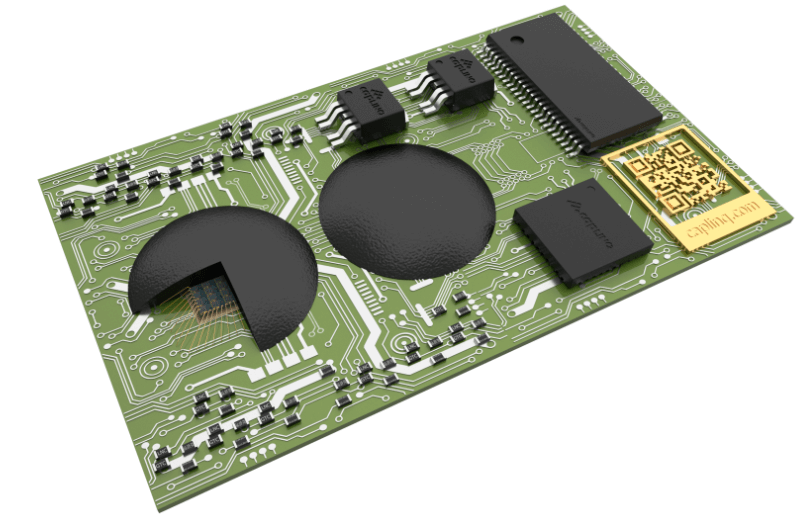
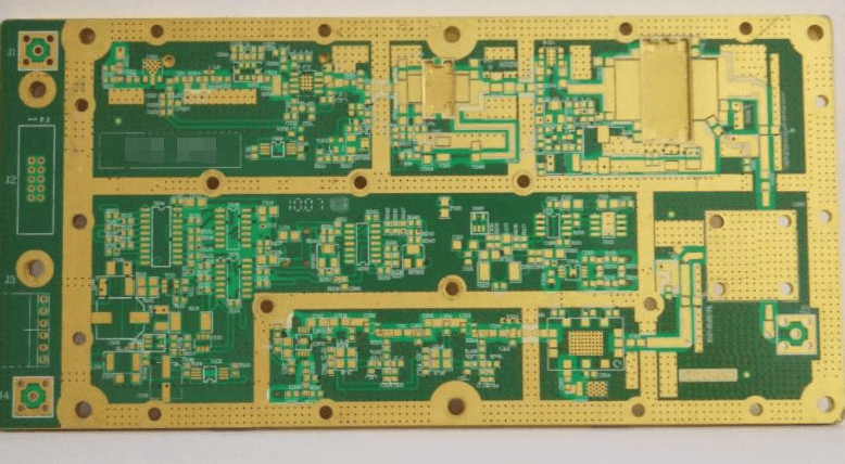
PCB chip packaging and welding
Chip on board (COB), semiconductors place chips on printed circuit boards and achieve electrical connections between chips and substrates through wire stitching. The electrical connection between the chip and the substrate is achieved through wire stitching and covered with resin to ensure reliability. . Although COB is the simplest chip-on-chip technology, its packaging density is much lower than TAB and flip chip bonding.
Chip on board (COB) The process first covers the wafer placement points on the substrate surface with thermally conductive epoxy (usually epoxy doped with silver particles), and then places the silicon wafer directly on the substrate surface and heats it to the silicon. The sheet is firmly fixed on the substrate, and then the electrical connection is directly established between the silicon wafer and the substrate through wire bonding.
Compared with other packaging technologies, COB technology is cheap (only about 1/3 of the same chip), space-saving, and mature technology. However, any new technology cannot be perfect when it first appears. COB technology also has the disadvantages of requiring additional welding machines and packaging machines, sometimes the speed cannot keep up, and the PCB patch is more stringent and cannot be repaired.
Chip-on-board (CoB) layouts can improve IC signal performance because they can remove most or all of the package, thereby eliminating most or all of the parasitic devices. However, some performance issues may occur using these techniques. In all of these designs, the substrate may not be well connected to VCC or ground due to the lead frame board or BGA markings. Possible problems include coefficient of thermal expansion (CTE) problems and poor substrate connection.
Main welding methods for COB:
(1) Thermal compression bonding
The solder wire is welded to the welding area by heating and applying pressure. The principle is that the heating area and pressure cause the welding area (such as AI) to plastically deform and destroy the oxide layer on the pressure welding interface, so that the attraction between atoms achieves the purpose of “bonding”. In addition, when the two metal interfaces are uneven, heating and pressure are applied, and the upper and lower metals can be inlaid with each other. This technology is commonly used as chip COG on glass.
(2) U ultrasonic welding
Ultrasonic welding uses energy generated by an ultrasonic generator. Through the magnetic field induction of the inverter at ultra-high frequency, it expands and contracts rapidly, generating elastic vibrations, causing the file to vibrate accordingly, and at the same time exerting a certain pressure on the file, so that the file is combined under the action of these two forces, the AI wire quickly rubs on the surface of the metallization layer, such as the (AI film) in the welding area, and the surface of the AI wire and the AI film undergo plastic deformation. . This deformation also destroys the interface of the AI layer. The oxide layer makes the two pure metal surfaces in close contact to achieve atomic bonding, thereby forming a weld. The main welding material is an aluminum welding wire welding head, which is usually wedge-shaped.
(3) Gold wire welding g
Ball bonding is the most representative welding technology in lead bonding, because the current semiconductor packaging diode and transistor packaging use AU wire ball bonding. In addition, it is easy to operate, flexible, and has a firm solder joint (AU wire with a diameter of 25 UM is usually 0.07 to 0.09 N/point), and has no directionality, and the welding speed can be as high as 15 minutes/second or more. Gold wire welding is also called hot (pressure) (super) ultrasonic welding. The main bonding material is gold (AU) wire bonding head is spherical, so it is ball bonding.

COB packaging process
Step1: Crystal expansion. The expansion of the entire LED chip film provided by the manufacturer is evenly expanded by the expander, so that the LED grains tightly attached to the surface of the film are pulled apart for easy puncture.
Step2: Adhesive. Put the crystal expansion ring with crystal expansion on the surface of the bonding machine, the silver paste layer and the silver paste on the back. Point silver paste. Apply to bulk LED chips. Use a dispenser to find the right amount of silver paste on the PCB printed circuit board.
Step 3: Insert the silver paste ring filled with crystal into the puncture frame, and the operator punctures the LED chip on the PCB printed circuit board with a lancet under a microscope.
Step 4: Put the perforated PCB printed circuit board into the thermal cycle oven for a period of time, and wait for the silver paste to solidify (not set for a long time, otherwise the LED chip coating will be baked yellow, that is, oxidized, and bonding will cause difficulties). If there is LED chip bonding, the above steps are required; if only IC chips are bonded, the above steps are cancelled.
Step 5: Paste the chip. Use a dispenser to apply an appropriate amount of red glue (or vinyl) to the IC position of the PCB printed circuit board, and then use an anti-static device (vacuum pen or sub) to correctly place the IC chip on the red or black glue.
Step 6: Drying. Place the bonded mold in a thermal cycle oven and place it on a large flat heating plate for a while, or it can be cured naturally (longer time).
Step 7: Bonding (wire). The wafer (LED chip or IC chip) is bridged with the corresponding pad aluminum wire on the PCB through an aluminum wire bonding machine, that is, the internal leads of the COB are welded.
Step 8: Pre-test. Use special inspection tools (COB has different equipment for different purposes, the simplest one is a high-precision regulated power supply) to detect the COB board and rework the unqualified board.
Step 9: Dispensing. The dispenser is equipped with an appropriate amount of AB glue to bond the LED die. The IC is packaged in black plastic and then packaged according to customer requirements.
Step 10: Curing. Put the sealed PCB printed circuit board into a thermal cycle oven to keep it at a constant temperature. Different drying times can be set according to requirements.
Step 11: Post-test. Then use a special detection tool to test the electrical performance of the packaged PCB printed circuit board to distinguish good from bad.