PCB Circuit Board Cleaning Technology and Step-by-Step Process Introduction
1. Introduction
Printed Circuit Boards (PCBs) are essential components in modern electronic devices. During manufacturing, assembly, and usage, PCBs can accumulate contaminants such as flux residues, dust, oils, and solder particles. These contaminants can lead to short circuits, corrosion, and reduced performance. Therefore, proper PCB cleaning is crucial to ensure reliability, longevity, and optimal functionality.
This article explores various PCB cleaning technologies, their advantages and disadvantages, and provides a detailed step-by-step guide to effective PCB cleaning.
2. Importance of PCB Cleaning
Cleaning PCBs is necessary for several reasons:
- Preventing Electrical Failures: Contaminants can cause short circuits or leakage currents.
- Enhancing Soldering Quality: Residual flux can weaken solder joints over time.
- Improving Thermal Performance: Dust and debris can obstruct heat dissipation.
- Ensuring Long-Term Reliability: Corrosion caused by ionic residues can degrade PCB performance.
- Meeting Industry Standards: Many industries (e.g., aerospace, medical, automotive) require high cleanliness levels.
3. Common PCB Contaminants
Before cleaning, it is essential to identify the types of contaminants:
- Flux Residues: Leftover from soldering (rosin-based, water-soluble, or no-clean flux).
- Solder Balls/Particles: Tiny solder fragments that may cause shorts.
- Dust and Debris: Accumulated during manufacturing or operation.
- Oils and Grease: From fingerprints or machinery.
- Oxidation and Corrosion: Due to exposure to moisture or chemicals.
4. PCB Cleaning Technologies
Several cleaning methods are available, each suited for different contamination levels and PCB types.
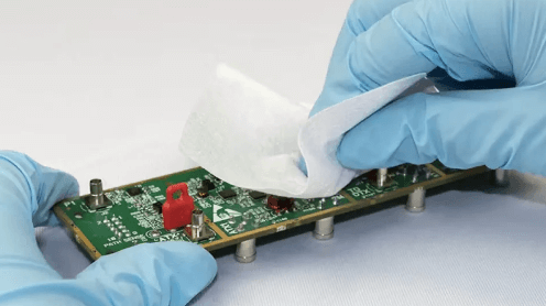
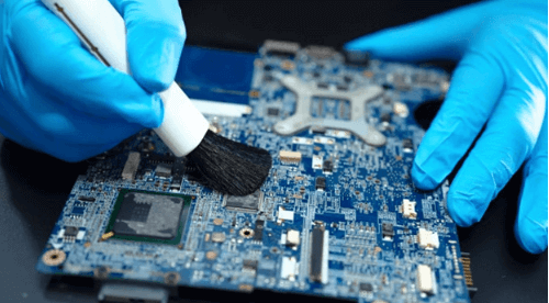
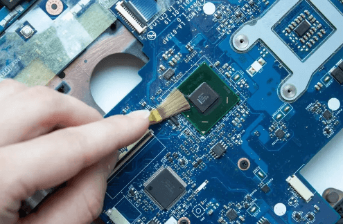
4.1. Manual Cleaning
Process: Using brushes, swabs, or lint-free cloths with cleaning solvents.
Pros:
- Low cost for small-scale cleaning.
- Suitable for spot cleaning.
Cons: - Labor-intensive.
- Risk of static damage or mechanical harm.
4.2. Ultrasonic Cleaning
Process: High-frequency sound waves create cavitation bubbles in a cleaning solution, removing contaminants.
Pros:
- Effective for complex geometries.
- Removes microscopic particles.
Cons: - May damage fragile components if improperly used.
- Requires proper solvent selection.
4.3. Vapor Degreasing
Process: PCBs are exposed to solvent vapors that condense and dissolve contaminants.
Pros:
- Fast and efficient.
- Minimal solvent waste.
Cons: - Limited to volatile solvents.
- Not suitable for water-soluble contaminants.
4.4. Aqueous Cleaning
Process: Uses water-based solutions with detergents, often combined with spray or immersion.
Pros:
- Environmentally friendly.
- Effective for removing ionic residues.
Cons: - Requires drying to prevent moisture damage.
- May not remove some stubborn fluxes.
4.5. Semi-Aqueous Cleaning
Process: Combines solvent and water rinsing for tough residues.
Pros:
- Balances effectiveness and safety.
- Good for mixed contaminant types.
Cons: - More complex process.
- Higher cost than pure aqueous or solvent cleaning.
4.6. Plasma Cleaning
Process: Uses ionized gas to remove organic residues at a microscopic level.
Pros:
- Ultra-precise cleaning.
- No chemical waste.
Cons: - Expensive equipment.
- Limited to specific applications.
5. Step-by-Step PCB Cleaning Process
The following steps outline a general PCB cleaning procedure:
Step 1: Inspection and Pre-Cleaning Assessment
- Visually inspect the PCB for contaminants.
- Identify the type of residues (flux, dust, etc.).
- Choose the appropriate cleaning method based on PCB sensitivity and contamination.
Step 2: Dry Cleaning (If Applicable)
- Use compressed air or a soft brush to remove loose dust and particles.
- Avoid excessive force to prevent component damage.
Step 3: Solvent Selection
- For flux residues: Isopropyl alcohol (IPA) or specialized flux removers.
- For oils/grease: Mild detergents or degreasers.
- For water-soluble residues: Deionized (DI) water or aqueous cleaners.
Step 4: Cleaning Application
- Manual Cleaning: Apply solvent with a brush or lint-free cloth, gently scrubbing.
- Ultrasonic Cleaning: Immerse PCB in a tank with cleaning solution (2-10 minutes).
- Spray Cleaning: Use a spray bottle or automated system for even coverage.
Step 5: Rinsing (If Required)
- For aqueous or semi-aqueous methods, rinse with DI water to remove cleaning agent traces.
- Ensure no residue remains.
Step 6: Drying
- Use compressed air to blow off excess liquid.
- Bake at low temperature (50-60°C) or use a drying oven for thorough moisture removal.
Step 7: Post-Cleaning Inspection
- Check for cleanliness under magnification.
- Perform electrical tests if necessary.
Step 8: Conformal Coating (Optional)
- Apply protective coating to prevent future contamination.
6. Safety and Environmental Considerations
- Ventilation: Ensure proper airflow when using solvents.
- Static Control: Use anti-static tools to prevent ESD damage.
- Waste Disposal: Follow regulations for chemical disposal.
- Material Compatibility: Avoid solvents that may damage PCB materials.
7. Conclusion
PCB cleaning is a critical step in ensuring the reliability and performance of electronic assemblies. Depending on the contamination type and PCB design, various cleaning methods—such as ultrasonic, aqueous, or vapor degreasing—can be employed. Following a structured cleaning process helps maintain high-quality standards and extends PCB lifespan.
As technology advances, eco-friendly and precision cleaning techniques will continue to evolve, offering better solutions for modern PCB manufacturing and maintenance.


