Pcb circuit design online
Top Online Tools For PCB Circuit Design
Printed Circuit Board (PCB) design is a critical aspect of modern electronics, and the advent of online tools has revolutionized the way engineers and hobbyists approach this task. These tools offer a range of functionalities that streamline the design process, making it more accessible and efficient. Among the top online tools for PCB circuit design, several stand out due to their comprehensive features, user-friendly interfaces, and robust support systems.
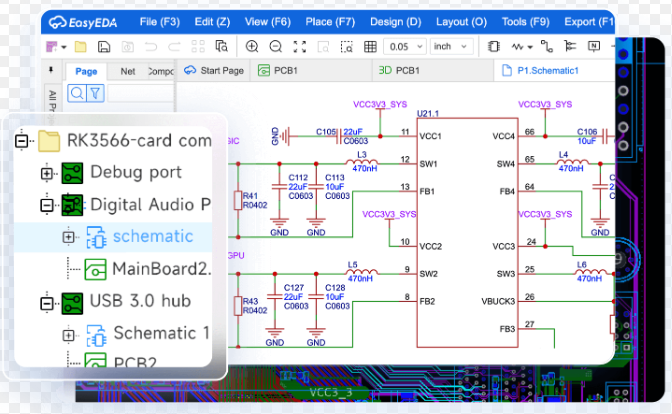
One of the most prominent online tools is EasyEDA.
This platform is highly regarded for its intuitive interface and extensive library of components.
EasyEDA allows users to design schematics, simulate circuits, and lay out PCBs all within a single environment. The tool supports collaboration, enabling multiple users to work on the same project simultaneously. Additionally, EasyEDA integrates seamlessly with LCSC, a major electronic component supplier, facilitating the procurement process. This integration ensures that designers can easily source the components they need, streamlining the transition from design to production.
Another noteworthy tool is KiCad, an open-source software suite that has gained significant traction in the PCB design community.
Although traditionally a desktop application, KiCad has expanded its capabilities to include online collaboration features. KiCad is known for its powerful schematic capture and PCB layout tools, which are suitable for both simple and complex designs. The software’s open-source nature means that it is continually being improved by a dedicated community of developers, ensuring that it remains at the cutting edge of PCB design technology.
For those seeking a more professional-grade tool, Altium 365 offers a cloud-based platform that brings the power of Altium Designer to the web.
Altium 365 provides advanced features such as real-time collaboration, version control, and seamless integration with mechanical design tools. This platform is particularly beneficial for teams working on large-scale projects, as it allows for efficient management of design data and facilitates communication between team members. The ability to access Altium Designer’s powerful features online makes Altium 365 a compelling choice for professional engineers.
In addition to these tools, Upverter is another online platform that deserves mention.
Upverter is designed with a focus on ease of use, making it an excellent choice for beginners and educators. The platform offers a range of tutorials and resources to help users get started with PCB design. Upverter’s collaborative features are also noteworthy, allowing users to share their designs with others and receive feedback in real-time. This makes it an ideal tool for educational settings, where students can learn from each other and from more experienced designers.
While each of these tools has its unique strengths, they all share the common goal of making PCB design more accessible and efficient.
The ability to design circuits online offers numerous advantages, including the convenience of accessing projects from any location, the ease of collaboration, and the integration with component suppliers. As technology continues to advance, it is likely that these tools will become even more powerful and user-friendly, further democratizing the field of PCB design.
In conclusion, the top online tools for PCB circuit design—EasyEDA, KiCad, Altium 365, and Upverter—each offer distinct features that cater to different needs and skill levels. Whether you are a hobbyist, a student, or a professional engineer, these tools provide the resources necessary to bring your electronic designs to life. The continued development and enhancement of these platforms promise to keep PCB design at the forefront of technological innovation.

Step-by-Step Guide To Designing PCBs Online
Designing printed circuit boards (PCBs) online has become increasingly accessible and efficient, thanks to advancements in software tools and resources. This step-by-step guide aims to provide a comprehensive overview of the process, ensuring that even those new to PCB design can navigate the complexities with ease.
To begin with, the initial step in designing a PCB online involves selecting the appropriate software.
Numerous platforms, such as KiCad, Eagle, and Altium Designer, offer robust features tailored to various levels of expertise. Once the software is chosen, the next phase is to conceptualize the circuit. This involves creating a schematic diagram, which serves as a blueprint for the PCB. The schematic diagram is a graphical representation of the electrical connections and components within the circuit. It is crucial to ensure that all components are correctly placed and connected, as this will directly impact the functionality of the final product.
Following the creation of the schematic, the next step is to define the board layout.
This involves translating the schematic diagram into a physical layout that can be manufactured. During this phase, it is essential to consider factors such as component placement, trace routing, and layer management. Proper component placement is vital for optimizing the performance and reliability of the PCB. Components should be arranged logically, with related parts placed in close proximity to minimize signal interference and reduce trace lengths.
Once the components are placed, the next task is to route the traces.
Trace routing involves creating the electrical pathways that connect the components on the PCB. This step requires careful planning to avoid issues such as signal crosstalk, electromagnetic interference, and impedance mismatches. Utilizing the software’s auto-router feature can expedite this process, although manual adjustments may be necessary to achieve optimal results. Additionally, it is important to adhere to design rules and constraints, which are typically provided by the PCB manufacturer. These rules ensure that the design meets the necessary specifications for fabrication and assembly.
After completing the trace routing, the next step is to perform a design rule check (DRC).
The DRC is a critical process that verifies the design against a set of predefined rules to identify potential errors or violations. This step helps to ensure that the PCB design is manufacturable and free of issues that could compromise its performance. Any errors identified during the DRC should be addressed promptly to avoid costly revisions later in the process.
With the design rule check completed, the final step is to generate the necessary files for manufacturing.
These files, commonly referred to as Gerber files, contain all the information required by the PCB manufacturer to produce the board. The Gerber files include details such as the copper layers, solder mask, silkscreen, and drill files. It is essential to review these files thoroughly to ensure accuracy before submitting them to the manufacturer.
In conclusion, designing PCBs online involves a series of methodical steps, from selecting the appropriate software and creating a schematic diagram to defining the board layout, routing traces, performing a design rule check, and generating manufacturing files. By following this step-by-step guide, designers can navigate the complexities of PCB design with confidence, ultimately producing high-quality, reliable circuit boards.
Common Mistakes To Avoid In Online PCB Design
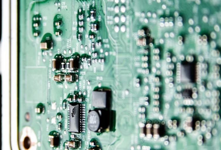
Designing printed circuit boards (PCBs) online has become increasingly accessible, thanks to the proliferation of sophisticated software tools. However, despite the convenience and advanced features these tools offer, there are common mistakes that designers, especially novices, often make. Avoiding these pitfalls is crucial for ensuring the functionality, reliability, and manufacturability of the final product.
One frequent mistake is neglecting to adhere to design rules and constraints.
Online PCB design tools typically come with built-in design rule checks (DRCs) that help ensure your layout meets specific manufacturing requirements. Ignoring these rules can lead to issues such as short circuits, insufficient spacing between components, and other manufacturing defects. Therefore, it is essential to familiarize yourself with the DRC settings and ensure they are correctly configured for your specific project.
Another common error is improper component placement.
Efficient component placement is vital for optimizing the performance and manufacturability of the PCB. Placing components too close together can lead to difficulties in soldering and increased risk of short circuits. Conversely, placing them too far apart can result in longer trace lengths, which may introduce signal integrity issues. To avoid these problems, it is advisable to follow best practices for component placement, such as grouping related components together and maintaining adequate spacing.
In addition to component placement, trace routing is another area where designers often falter.
Poor trace routing can lead to a host of issues, including signal interference, impedance mismatches, and increased electromagnetic interference (EMI). To mitigate these risks, it is important to follow guidelines for trace width, spacing, and routing paths. For instance, keeping high-speed signal traces as short and direct as possible can help minimize signal degradation. Additionally, using ground planes and proper shielding techniques can significantly reduce EMI.
Thermal management is another critical aspect that is often overlooked in online PCB design.
Components generate heat during operation, and inadequate thermal management can lead to overheating and potential failure. To address this, designers should consider the thermal properties of the materials used and incorporate features such as thermal vias, heat sinks, and adequate ventilation. Conducting thermal simulations can also provide valuable insights into potential hotspots and help in making informed design decisions.
Furthermore, failing to perform thorough design reviews and simulations is a mistake that can have costly repercussions.
Online PCB design tools offer various simulation features, such as signal integrity analysis, power integrity analysis, and thermal simulations. Utilizing these features can help identify potential issues early in the design process, thereby reducing the likelihood of costly revisions later. Regular design reviews, involving multiple stakeholders, can also provide diverse perspectives and help catch errors that might have been overlooked.
Lastly, documentation is an often-neglected aspect of PCB design.
Comprehensive documentation, including schematics, layout files, bill of materials (BOM), and assembly instructions, is essential for successful manufacturing and assembly. Incomplete or inaccurate documentation can lead to misunderstandings and errors during production. Therefore, it is crucial to ensure that all design files are well-documented and up-to-date.
In conclusion, while online PCB design tools offer numerous advantages, it is important to be aware of and avoid common mistakes to ensure a successful outcome. By adhering to design rules, optimizing component placement and trace routing, managing thermal properties, performing thorough reviews and simulations, and maintaining comprehensive documentation, designers can significantly enhance the quality and reliability of their PCB designs.
Benefits Of Using Online Platforms For PCB Prototyping
The advent of online platforms for PCB (Printed Circuit Board) prototyping has revolutionized the electronics industry, offering numerous benefits that streamline the design and manufacturing process. One of the most significant advantages is the accessibility these platforms provide. Engineers and hobbyists alike can access sophisticated design tools from virtually anywhere, eliminating the need for expensive, specialized software. This democratization of technology allows for a broader range of individuals to engage in PCB design, fostering innovation and creativity.
Moreover, online platforms often come equipped with user-friendly interfaces and comprehensive libraries of components, which significantly reduce the learning curve for beginners.
These libraries are regularly updated to include the latest components, ensuring that designers have access to the most current technology. Additionally, many platforms offer tutorials and community forums where users can seek advice and share knowledge, further enhancing the learning experience.
Another key benefit is the efficiency and speed of the design process.
Traditional PCB prototyping can be time-consuming, often requiring multiple iterations and physical prototypes before achieving the desired outcome. In contrast, online platforms enable rapid prototyping through advanced simulation tools that allow designers to test and validate their circuits virtually. This capability not only accelerates the development cycle but also reduces the risk of errors, as potential issues can be identified and addressed early in the design phase.
Cost-effectiveness is another compelling advantage of using online platforms for PCB prototyping.
The traditional approach often involves significant upfront investment in software licenses, hardware, and materials. Online platforms, however, typically operate on a subscription or pay-per-use model, making them more affordable for small businesses and individual designers. Furthermore, the ability to simulate and test designs virtually reduces the need for physical prototypes, thereby lowering material costs and minimizing waste.
Collaboration is also greatly enhanced through the use of online platforms
In today’s globalized world, design teams are often dispersed across different locations. Online PCB design tools facilitate seamless collaboration by allowing multiple users to work on the same project simultaneously. Features such as version control and real-time updates ensure that all team members are on the same page, thereby improving communication and reducing the likelihood of errors.
In addition to these practical benefits, online platforms also contribute to the sustainability of the electronics industry.
By reducing the need for physical prototypes and minimizing material waste, these tools support more environmentally friendly design practices. This is particularly important in an era where sustainability is becoming a key consideration for businesses and consumers alike.
Furthermore, the integration of online platforms with manufacturing services offers a streamlined path from design to production.
Many platforms have partnerships with PCB manufacturers, allowing users to order their designs directly from the platform. This integration not only simplifies the ordering process but also ensures that the final product meets the specifications outlined in the design, thereby reducing the risk of discrepancies and defects.
In conclusion, the benefits of using online platforms for PCB prototyping are manifold, ranging from increased accessibility and efficiency to cost savings and enhanced collaboration. These platforms are transforming the way PCBs are designed and manufactured, making the process more inclusive, efficient, and sustainable. As technology continues to evolve, it is likely that the capabilities of these platforms will only expand, further solidifying their role as indispensable tools in the field of electronics design.