PCB Component Image Segmentation Methods: A Comprehensive Review
Abstract
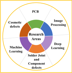
Printed Circuit Board (PCB) component image segmentation is a critical task in automated optical inspection (AOI), quality control, and reverse engineering of electronic circuits. This paper provides a comprehensive review of various image segmentation techniques applied to PCB component images, discussing traditional approaches, machine learning-based methods, and deep learning architectures. We examine the challenges specific to PCB component segmentation, evaluate performance metrics, and discuss current limitations and future research directions in this specialized field of computer vision.
Keywords: PCB, image segmentation, component recognition, deep learning, computer vision
1. Introduction
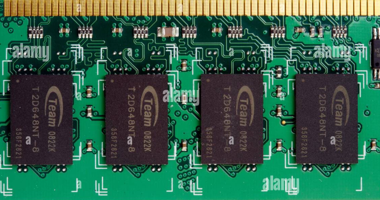
Printed Circuit Boards (PCBs) form the backbone of modern electronic devices, containing complex arrangements of components that must be accurately manufactured and inspected. Automated visual inspection of PCBs relies heavily on robust image segmentation techniques to identify and isolate individual components from the board’s background and from each other.
PCB component image segmentation presents unique challenges due to:
- High component density with varying sizes and shapes
- Reflective surfaces causing specular highlights
- Color similarities between components and substrate
- Occlusions from irregular component shapes
- Variations in lighting conditions during image acquisition
Traditional segmentation approaches often struggle with these challenges, leading to the development of specialized techniques for PCB analysis. This paper systematically reviews these methods, organized by their underlying technical approaches.
2. Traditional Image Segmentation Methods for PCB Components
2.1 Threshold-based Techniques
Global and adaptive thresholding methods have been widely applied to PCB images:
Otsu’s method (Otsu, 1979) automatically determines optimal threshold values by maximizing inter-class variance. While effective for high-contrast PCB images, it struggles with:
- Low contrast between components and substrate
- Non-uniform illumination
- Color components that don’t separate well in grayscale
Adaptive thresholding techniques like Sauvola’s method (Sauvola & Pietikäinen, 2000) perform better with illumination variations by computing local thresholds within sliding windows.
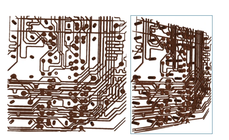
2.2 Edge-based Segmentation
Edge detection operators (Canny, Sobel, Prewitt) identify component boundaries:
Canny edge detection remains popular for PCB analysis due to its noise resistance. However, challenges include:
- Broken edges at low-contrast regions
- False edges from text and PCB traces
- Difficulty closing complete component contours
Edge linking algorithms are often required as post-processing to form closed boundaries.
2.3 Region-based Methods
Region growing starts from seed points and merges neighboring pixels with similar properties. For PCBs:
- Effective for homogeneous components (e.g., large ICs)
- Struggles with textured components (e.g., capacitors)
- Sensitive to seed placement
Watershed transformation (Vincent & Soille, 1991) treats image intensity as topography:
- Useful for separating touching components
- Prone to over-segmentation from noise
- Often requires marker-controlled variants for PCBs
2.4 Color-based Segmentation
Color spaces (HSV, Lab) can improve segmentation of colored components:
K-means clustering in color spaces helps group similar components but requires:
- Careful selection of K values
- Color space transformation choices
- Post-processing to merge oversegmented regions
3. Machine Learning Approaches
3.1 Feature Engineering + Classifiers
Traditional ML pipelines for PCB segmentation involve:
- Feature extraction: Texture (LBP, Haralick), shape (Hu moments), color histograms
- Classifier training: SVM, Random Forests, AdaBoost
- Pixel-wise classification
Limitations include:
- Manual feature engineering requirements
- Poor generalization across different PCB types
- Difficulty handling component variations
3.2 Conditional Random Fields (CRFs)
CRFs model contextual relationships between pixels:
- Effective for post-processing segmentation results
- Can incorporate spatial and color information
- Computationally expensive for high-res PCB images
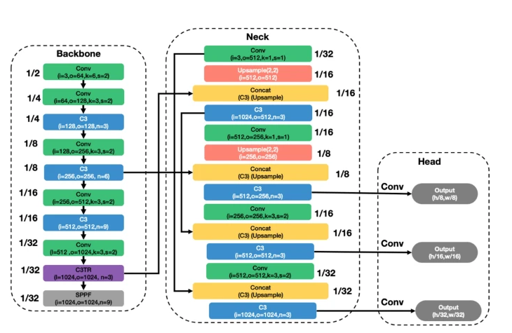
4. Deep Learning-Based Segmentation
4.1 Convolutional Neural Networks (CNNs)
Fully Convolutional Networks (FCNs) and their variants have revolutionized PCB segmentation:
U-Net (Ronneberger et al., 2015) architecture advantages:
- Skip connections preserve spatial details
- Effective with limited training data
- Good for small PCB components
Modifications for PCB segmentation:
- Attention mechanisms for important regions
- Dense connections for feature reuse
- Depthwise separable convolutions for efficiency
4.2 Instance Segmentation Architectures
Mask R-CNN (He et al., 2017) provides both detection and segmentation:
- Precise component boundaries
- Handles overlapping components
- Requires extensive bounding box annotations
YOLO variants with segmentation heads offer real-time capability important for inline inspection.
4.3 Transformer-based Approaches
Vision Transformers (ViTs) and hybrid architectures:
- Swin Transformer for hierarchical feature learning
- TransUNet combining transformers with U-Net
- Better long-range dependency modeling than CNNs
5. PCB-Specific Challenges and Solutions
5.1 Small Component Segmentation
Techniques for tiny components (0402, 0201 packages):
- High-resolution input patches
- Feature pyramid networks
- Attention to small regions
5.2 Reflective Surface Handling
Approaches for shiny components:
- Polarized lighting during acquisition
- Specular highlight detection and inpainting
- Data augmentation with synthetic reflections
5.3 Occlusion Handling
For partially hidden components:
- Context-aware segmentation
- Multi-view imaging
- 3D reconstruction approaches
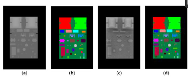
6. Evaluation Metrics and Performance
Common metrics for PCB segmentation:
- Pixel accuracy: Basic but misleading for class imbalance
- IoU (Jaccard Index): More informative for component shapes
- Dice coefficient: Similar to IoU but more emphasis on overlap
- Boundary F1 score: For edge quality assessment
State-of-the-art performance (representative studies):
- Deep learning methods achieve >95% Dice on clean images
- Drops to 80-90% for challenging cases (small, reflective components)
- Traditional methods typically below 80% for complex PCBs
7. Datasets and Annotation
Public PCB segmentation datasets:
- PCBComponent: 5,000 images with 12 component categories
- FICS-PCB: Includes segmentation masks for ICs
- DeepPCB: Focused on defects but useful for component study
Annotation challenges:
- Precise boundary demarcation
- Component categorization
- Handling overlapping instances
8. Industrial Applications
8.1 Automated Optical Inspection (AOI)
- Component presence/absence verification
- Polarity checking
- Tombstoning detection
8.2 Quality Control
- Solder joint inspection
- Component placement accuracy
- Size and shape verification
8.3 Reverse Engineering
- Component extraction for board analysis
- Circuit reconstruction
- BOM generation
9. Limitations and Future Directions
Current challenges:
- Limited annotated datasets
- Generalization across PCB types
- Real-time processing requirements
Future research directions:
- Self-supervised learning for PCB segmentation
- Few-shot learning for new components
- Multimodal approaches (combining visual, thermal, x-ray)
- Edge-optimized models for factory deployment
10. Conclusion
PCB component image segmentation has evolved significantly from traditional image processing techniques to sophisticated deep learning architectures. While current methods achieve good performance in controlled conditions, challenges remain in handling real-world variability, tiny components, and reflective surfaces. The future of PCB segmentation lies in more robust architectures, better datasets, and efficient implementations suitable for industrial deployment. Continued advancements in this field will directly contribute to improved quality and reliability in electronics manufacturing.