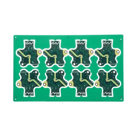
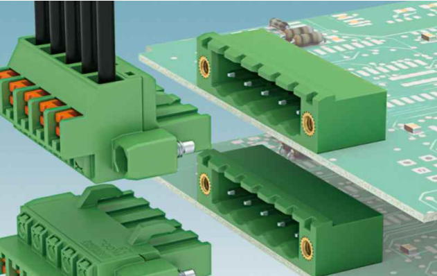
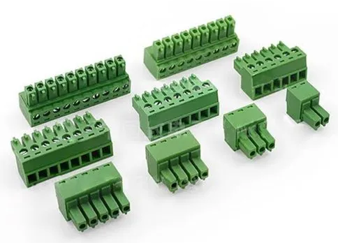
Pcb connector high frequency
Optimizing PCB Connector Design for High-Frequency Applications
In the realm of modern electronics, the demand for high-frequency applications is ever-increasing, necessitating the optimization of printed circuit board (PCB) connector designs. High-frequency signals, typically defined as those operating at frequencies above 1 GHz, present unique challenges that require meticulous attention to detail in the design and implementation of PCB connectors. The primary objective is to ensure signal integrity, minimize losses, and reduce electromagnetic interference (EMI), all of which are critical for the reliable performance of high-frequency electronic systems.
To begin with, the choice of materials plays a pivotal role in optimizing PCB connectors for high-frequency applications.
Conductive materials with low resistivity, such as copper or gold, are preferred for their excellent electrical conductivity. Additionally, dielectric materials with low permittivity and loss tangent are essential to minimize signal attenuation and dispersion. These materials help maintain the integrity of high-frequency signals as they traverse the PCB connectors.
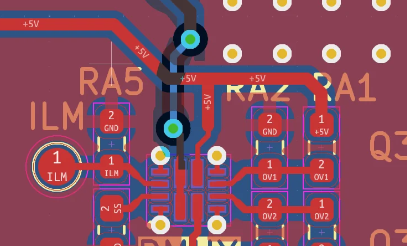
Furthermore, the physical design of the connectors must be carefully considered.
The geometry of the connectors, including the length, width, and spacing of the conductive traces, directly impacts the impedance and signal integrity. Impedance matching is crucial to prevent signal reflections, which can cause significant degradation in high-frequency applications. Therefore, precise control over the dimensions and layout of the connectors is necessary to achieve the desired impedance characteristics.
In addition to material selection and physical design, the implementation of shielding techniques is vital for mitigating EMI.
High-frequency signals are particularly susceptible to interference from external sources, which can lead to signal degradation and data loss. Shielding can be achieved through the use of ground planes, metal enclosures, or conductive coatings that surround the connectors. These measures help to isolate the high-frequency signals from external noise sources, thereby preserving signal integrity.
Moreover, the integration of differential signaling techniques can enhance the performance of PCB connectors in high-frequency applications.
Differential signaling involves the use of two complementary signals that are transmitted simultaneously. This approach helps to cancel out common-mode noise and reduces susceptibility to EMI. By employing differential pairs, designers can achieve higher data rates and improved signal integrity, which are essential for high-frequency applications.
Thermal management is another critical aspect that must be addressed in the design of PCB connectors for high-frequency applications.
High-frequency signals can generate significant heat, which can adversely affect the performance and reliability of the connectors. Effective thermal management strategies, such as the use of heat sinks, thermal vias, and conductive cooling materials, are necessary to dissipate heat and maintain optimal operating temperatures.
Furthermore, the manufacturing process must be meticulously controlled to ensure the precision and reliability of high-frequency PCB connectors.
Advanced fabrication techniques, such as laser drilling and precision etching, are often employed to achieve the required tolerances and geometries. Quality control measures, including rigorous testing and inspection, are essential to verify the performance and integrity of the connectors.
In conclusion, optimizing PCB connector design for high-frequency applications involves a multifaceted approach that encompasses material selection, physical design, shielding, differential signaling, thermal management, and precise manufacturing processes. By addressing these critical factors, designers can ensure the reliable performance of high-frequency electronic systems, thereby meeting the growing demands of modern technology. The continuous advancement in PCB connector design will undoubtedly play a pivotal role in the evolution of high-frequency applications, driving innovation and enabling new possibilities in the field of electronics.

Material Selection for High-Frequency PCB Connectors
When designing high-frequency printed circuit board (PCB) connectors, material selection plays a pivotal role in ensuring optimal performance and reliability. The choice of materials directly impacts the electrical, thermal, and mechanical properties of the connectors, which are critical in high-frequency applications. Therefore, understanding the characteristics and suitability of various materials is essential for engineers and designers.
One of the primary considerations in material selection for high-frequency PCB connectors is the dielectric constant (Dk) of the substrate material.
A low dielectric constant is preferred as it reduces signal loss and ensures signal integrity at high frequencies. Materials such as polytetrafluoroethylene (PTFE), commonly known as Teflon, and other advanced laminates like Rogers materials are often chosen for their low Dk values. These materials provide excellent electrical insulation and minimal signal distortion, making them ideal for high-frequency applications.
In addition to the dielectric constant, the dissipation factor (Df) of the material is another crucial parameter.
The dissipation factor measures the energy loss as heat within the dielectric material. A low dissipation factor is desirable as it minimizes signal attenuation and power loss. PTFE and certain ceramic-filled laminates exhibit low dissipation factors, making them suitable for high-frequency PCB connectors where maintaining signal strength is paramount.
Thermal management is another critical aspect to consider when selecting materials for high-frequency PCB connectors.
High-frequency signals can generate significant heat, which, if not properly managed, can lead to performance degradation and potential failure of the connectors. Materials with high thermal conductivity, such as certain ceramics and metal composites, are often used to dissipate heat effectively. Additionally, these materials should have a low coefficient of thermal expansion (CTE) to ensure dimensional stability and prevent mechanical stress during thermal cycling.
Mechanical properties, including strength, flexibility, and durability, are also important factors in material selection.
High-frequency PCB connectors must withstand mechanical stresses during assembly, operation, and maintenance. Materials such as liquid crystal polymer (LCP) and certain high-performance thermoplastics offer excellent mechanical properties, including high tensile strength and resistance to wear and tear. These materials ensure the connectors maintain their structural integrity and performance over time.
Furthermore, the choice of conductive materials for the connector contacts is equally important.
Copper and its alloys are commonly used due to their excellent electrical conductivity and relatively low cost. However, for high-frequency applications, the skin effect becomes significant, where high-frequency currents tend to flow on the surface of the conductor. To mitigate this, surface treatments such as gold or silver plating are often applied to the contacts. These coatings provide a low-resistance path for high-frequency signals, ensuring minimal signal loss and improved performance.
Environmental considerations, such as resistance to moisture, chemicals, and temperature extremes, also influence material selection.
High-frequency PCB connectors may be exposed to harsh environments, and materials with high resistance to environmental factors are essential to ensure long-term reliability. For instance, PTFE and certain high-performance polymers exhibit excellent chemical resistance and stability under a wide range of temperatures, making them suitable for demanding applications.
In conclusion, the selection of materials for high-frequency PCB connectors is a multifaceted process that requires careful consideration of electrical, thermal, mechanical, and environmental properties. By choosing materials with low dielectric constants, low dissipation factors, high thermal conductivity, and robust mechanical properties, engineers can design connectors that meet the stringent demands of high-frequency applications. Additionally, surface treatments and environmental resistance further enhance the performance and reliability of these connectors, ensuring they function optimally in various conditions.
Challenges in High-Frequency PCB Connector Integration
Integrating high-frequency PCB connectors into electronic systems presents a myriad of challenges that engineers must navigate to ensure optimal performance and reliability. As electronic devices continue to evolve, the demand for high-speed data transmission and increased signal integrity has become paramount. High-frequency PCB connectors, which are essential for facilitating these requirements, introduce several complexities that must be meticulously addressed.
One of the primary challenges in high-frequency PCB connector integration is signal integrity.
At high frequencies, even minor imperfections in the connector design or PCB layout can lead to significant signal degradation. This degradation manifests as increased insertion loss, return loss, and crosstalk, which can severely impact the performance of the entire system. To mitigate these issues, engineers must employ advanced simulation tools and meticulous design practices. Ensuring that the impedance of the connector matches that of the transmission line is crucial, as impedance mismatches can cause reflections and signal loss.
Another significant challenge is the physical design and material selection for high-frequency connectors.
The materials used must exhibit low dielectric loss and high thermal stability to maintain signal integrity at elevated frequencies. Additionally, the physical dimensions of the connectors must be precisely controlled to avoid introducing parasitic inductance and capacitance, which can further degrade signal quality. The miniaturization trend in modern electronics exacerbates this challenge, as smaller connectors are more susceptible to these parasitic effects.
Thermal management also poses a considerable challenge in high-frequency PCB connector integration.
High-frequency signals generate more heat due to increased power dissipation, and this heat must be effectively managed to prevent damage to the connectors and surrounding components. Engineers must design efficient thermal pathways and consider the use of advanced cooling techniques, such as heat sinks or active cooling systems, to maintain the integrity of the connectors under high thermal loads.
Electromagnetic interference (EMI) is another critical concern when integrating high-frequency PCB connectors.
High-frequency signals are more prone to EMI, which can disrupt the operation of nearby electronic components and degrade overall system performance. Shielding and grounding techniques must be carefully implemented to minimize EMI. This often involves the use of specialized connector designs that incorporate shielding features, as well as meticulous PCB layout practices to ensure proper grounding and isolation of high-frequency signals.
Manufacturing tolerances and quality control are also pivotal in the successful integration of high-frequency PCB connectors.
The precision required in the manufacturing process is significantly higher than that for lower-frequency applications. Any deviations from the specified dimensions or material properties can lead to performance issues. Therefore, stringent quality control measures must be in place to ensure that each connector meets the required specifications. This often involves advanced inspection techniques, such as X-ray imaging and automated optical inspection, to detect and rectify any defects.
In conclusion, the integration of high-frequency PCB connectors into electronic systems is fraught with challenges that require a comprehensive and meticulous approach. Signal integrity, material selection, thermal management, EMI mitigation, and manufacturing precision are all critical factors that must be addressed to ensure the successful deployment of high-frequency connectors. As technology continues to advance, the demand for high-frequency connectors will only increase, necessitating ongoing innovation and refinement in design and manufacturing practices. By understanding and addressing these challenges, engineers can develop robust solutions that meet the ever-growing demands of modern electronic systems.
Testing and Validation Techniques for High-Frequency PCB Connectors
Testing and validation techniques for high-frequency PCB connectors are critical to ensuring the reliability and performance of electronic systems operating at elevated frequencies. As the demand for faster data transmission and higher signal integrity continues to grow, the importance of rigorous testing methodologies cannot be overstated. To begin with, one of the primary techniques employed in the validation of high-frequency PCB connectors is Time Domain Reflectometry (TDR). TDR is instrumental in identifying impedance mismatches, discontinuities, and other anomalies that could potentially degrade signal quality. By sending a fast rise-time pulse through the connector and analyzing the reflected signals, engineers can pinpoint the exact location and nature of any issues, thereby facilitating targeted corrective actions.
In addition to TDR, Vector Network Analysis (VNA) is another cornerstone technique in the validation process.
VNA measures the scattering parameters (S-parameters) of the PCB connectors, providing a comprehensive understanding of their behavior across a wide frequency range. This technique is particularly valuable for characterizing insertion loss, return loss, and crosstalk, which are critical parameters in high-frequency applications. By analyzing these metrics, engineers can assess the overall performance of the connectors and make informed decisions about their suitability for specific applications.
Moreover, Signal Integrity (SI) analysis plays a pivotal role in the testing and validation of high-frequency PCB connectors.
SI analysis involves the use of simulation tools to model the electrical performance of the connectors under various operating conditions. This approach allows engineers to predict potential issues such as signal degradation, jitter, and electromagnetic interference (EMI) before physical prototypes are built. By identifying and addressing these issues early in the design phase, the likelihood of costly redesigns and delays is significantly reduced.
Thermal testing is another essential aspect of the validation process.
High-frequency PCB connectors often operate in environments where temperature fluctuations can impact their performance. Thermal testing involves subjecting the connectors to a range of temperatures to evaluate their thermal stability and reliability. This testing ensures that the connectors can maintain their electrical performance and mechanical integrity under varying thermal conditions, which is crucial for applications in aerospace, automotive, and other demanding industries.
Furthermore, mechanical testing is conducted to assess the durability and robustness of high-frequency PCB connectors.
This includes tests for vibration, shock, and mechanical stress, which simulate real-world conditions that the connectors may encounter during their operational life. By evaluating the connectors’ mechanical resilience, engineers can ensure that they will perform reliably even in harsh environments.
Lastly, compliance testing with industry standards and regulations is a critical step in the validation process.
High-frequency PCB connectors must adhere to specific standards such as those set by the Institute of Electrical and Electronics Engineers (IEEE) and the International Electrotechnical Commission (IEC). Compliance testing ensures that the connectors meet the required performance criteria and are compatible with other components in the system. This step is essential for achieving certification and market acceptance.
In conclusion, the testing and validation of high-frequency PCB connectors involve a multifaceted approach that encompasses TDR, VNA, SI analysis, thermal testing, mechanical testing, and compliance testing. Each of these techniques provides valuable insights into the performance and reliability of the connectors, ensuring that they meet the stringent requirements of modern high-frequency applications. By employing these rigorous testing methodologies, engineers can deliver high-quality connectors that contribute to the overall success of electronic systems.