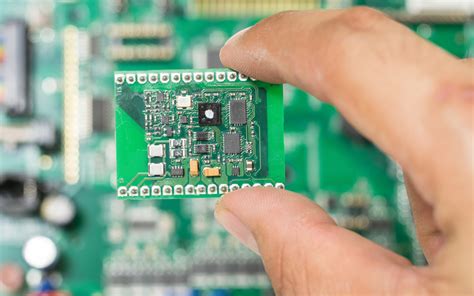
PCB Cooling Technology and Heat Dissipation of IC Packages
IC packages rely on PCBs to dissipate heat. Generally speaking, PCBs are the primary cooling method for high-power semiconductor devices. A good PCB thermal design can have a huge impact on the system’s good operation or the potential for thermal accidents. Careful handling of PCB layout, board structure, and device mounting can help improve the thermal performance of medium- and high-power applications.
Semiconductor manufacturing companies have little control over the systems in which their devices are used.
However, the system in which the IC is installed is critical to the overall device performance. For custom IC devices, system designers usually work closely with the manufacturer to ensure that the system meets the many thermal requirements of high-power devices. This early collaboration ensures that the IC meets electrical and performance standards while ensuring that it operates properly within the customer’s thermal system. Many large semiconductor companies sell devices as standard parts, and there is no contact between the manufacturer and the end application. In this case, we can only use some general guidelines to help achieve a good IC and system passive thermal solution.
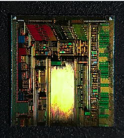
Common semiconductor package types are bare pad or PowerPADTM packages.
In these packages, the chip is mounted on a metal sheet called a chip pad. This die pad supports the chip during processing and also serves as a good thermal path for the device to dissipate heat. When the package’s exposed pad is soldered to the PCB, heat can quickly dissipate from the package and into the PCB. The heat is then dissipated through the PCB layers and into the surrounding air. Exposed pad packages typically conduct about 80% of the heat, which enters the PCB through the bottom of the package. The remaining 20% of the heat is dissipated through the device leads and the various sides of the package. Less than 1% of the heat is dissipated through the top of the package. For these exposed pad packages, good PCB thermal design is critical to ensure certain device performance.
The first aspect of PCB design that can improve thermal performance is PCB device layout.
Whenever possible, high-power components on the PCB should be separated from each other. This physical separation between high-power components maximizes the PCB area around each high-power component, which helps achieve better thermal conduction. Care should be taken to isolate temperature-sensitive components from high-power components on the PCB. Whenever possible, high power dissipation components should be mounted away from PCB corners. A more central PCB location maximizes the board area around the high power dissipation components, which helps dissipate heat. Figure 2 shows two identical semiconductor devices: components A and B. Component A, located at the corner of the PCB, has a 5% higher die junction temperature than component B, which is located more centrally. Heat dissipation at the corner of component A is limited because there is less board area around the component to dissipate heat.
The second area that has the most decisive influence on the thermal performance of a PCB design is the structure of the PCB.
As a general rule, the more copper a PCB has, the better the thermal performance of the system components. The ideal heat dissipation of a semiconductor device is with the die mounted on a large block of liquid-cooled copper. This mounting method is not practical for most applications, so other changes to the PCB are required to improve thermal performance. For most applications today, the shrinking overall system size has a negative impact on thermal performance. Larger PCBs have more area available for heat transfer, and more flexibility to leave enough space between high-power components.
Whenever possible, maximize the number and thickness of PCB copper ground planes.
Ground plane copper is generally heavier and is an excellent thermal path for heat dissipation throughout the PCB. Routing the layers also increases the total weight of copper available for heat transfer. However, this routing is usually done with electrical and thermal isolation, limiting its role as a potential heat sink. Routing the device ground plane to be as electrically similar as possible to many ground planes can help maximize thermal transfer. Thermal vias on the PCB under the semiconductor device help heat enter the buried layers of the PCB and conduct to the back of the board.
The top and bottom layers of the PCB are “golden areas” for improving thermal performance.
Using wider traces and routing away from high-power devices can provide a thermal path for heat dissipation. Specialized thermal pads are an excellent way to dissipate heat from the PCB. The thermal pad is typically located on the top or back of the PCB and is thermally connected to the device through direct copper connections or thermal vias. In the case of an inline package (a package with leads on only two sides), this pad can be located on the top of the PCB and shaped like a “dog bone” (narrow in the middle as the package, with a larger copper area away from the package, smaller in the middle and larger at the ends). In the case of a quad package (with leads on all four sides), the pad must be located on the back of the PCB or inside the PCB.
Increasing the size of the thermal pad is an excellent way to improve the thermal performance of a PowerPAD package. Different pad sizes have a significant impact on thermal performance.
Product data sheets that provide these dimensions are generally listed in a table format. However, it is difficult to quantify the impact of additional copper on a custom PCB.
Some online calculators allow users to select a device and then vary the size of the copper pad to estimate the impact on the thermal performance of a non-JEDEC PCB. These calculation tools highlight the extent to which PCB design can affect thermal performance. For quad packages, the top pad area is just smaller than the exposed pad area of the device, in which case buried or back layers are the first approach to achieve better cooling. For dual in-line packages, we can use a “dog bone” pad pattern to dissipate heat.

Finally, systems with larger PCBs can also be used for cooling.
Some of the screws used to mount the PCB can also become an effective thermal path to the base of the system when screw heatsinks are connected to the thermal pad and ground plane. Considering the thermal conductivity and cost, the number of screws should be the maximum to reach the point of diminishing returns. Metal PCB stiffeners have more cooling area after connecting to the thermal pad. For some applications where the PCB is covered with an enclosure, shape-controlled solder fill material has higher thermal performance than air-cooled enclosures. Cooling solutions such as fans and heat sinks are also common methods for system cooling, but they usually require more space or require design modifications to optimize cooling.
To design a system with high thermal performance, it is far from enough to just choose a good IC device and enclosure solution. The thermal performance of the IC depends on the PCB and the ability of the heat dissipation system to quickly cool the IC device. Using the above passive cooling method, the thermal performance of the system can be greatly improved.