Pcb copper
Benefits Of Using High-Quality Pcb copper Manufacturing
The utilization of high-quality copper in printed circuit board (PCB) manufacturing offers numerous benefits that significantly enhance the performance, reliability, and longevity of electronic devices. As the backbone of modern electronics, PCBs require materials that can efficiently conduct electricity while maintaining structural integrity. High-quality copper, known for its excellent electrical conductivity and thermal properties, plays a crucial role in meeting these demands.
One of the primary advantages of using high-quality copper in PCB manufacturing is its superior electrical conductivity.
Copper’s ability to conduct electricity with minimal resistance ensures that electronic signals are transmitted efficiently across the board. This is particularly important in high-frequency applications where signal integrity is paramount. By minimizing signal loss and reducing the risk of interference, high-quality copper helps maintain the performance of complex electronic systems, from consumer electronics to industrial machinery.
In addition to its electrical properties, high-quality copper also offers excellent thermal conductivity.
Effective heat dissipation is essential in preventing overheating and ensuring the longevity of electronic components. High-quality copper can efficiently transfer heat away from critical areas, reducing the risk of thermal damage and improving the overall reliability of the PCB. This is especially beneficial in high-power applications where managing heat is a significant concern.
Moreover, the mechanical properties of high-quality copper contribute to the durability and robustness of PCBs.
Copper’s malleability allows it to be easily shaped and formed into intricate patterns required for complex circuit designs. This flexibility, combined with its strength, ensures that the copper layers can withstand the mechanical stresses encountered during manufacturing and operation. Consequently, PCBs made with high-quality copper are less prone to cracking, delamination, and other forms of mechanical failure.
Furthermore, the use of high-quality copper in PCBs can lead to improved manufacturing processes and cost efficiencies.
High-quality copper materials often exhibit consistent thickness and purity, which simplifies the fabrication process and reduces the likelihood of defects. This consistency translates to higher yields and lower production costs, as fewer boards need to be discarded due to quality issues. Additionally, the enhanced performance and reliability of PCBs made with high-quality copper can reduce the need for costly repairs and replacements over the product’s lifecycle.
Another significant benefit of high-quality copper in PCB manufacturing is its environmental impact.
Copper is a recyclable material, and using high-quality copper can contribute to more sustainable manufacturing practices. By ensuring that the copper used in PCBs is of high quality, manufacturers can reduce waste and promote the recycling of materials, aligning with global efforts to minimize the environmental footprint of electronic devices.
In conclusion, the benefits of using high-quality copper in PCB manufacturing are multifaceted, encompassing improved electrical and thermal performance, enhanced mechanical properties, cost efficiencies, and environmental sustainability. As electronic devices continue to evolve and become more complex, the demand for reliable and efficient PCBs will only increase. By prioritizing the use of high-quality copper, manufacturers can ensure that their products meet the highest standards of performance and reliability, ultimately benefiting both consumers and the industry as a whole.
Techniques For Effective Copper Plating In PCB Design
Effective copper plating in printed circuit board (PCB) design is a critical aspect that significantly influences the performance, reliability, and longevity of electronic devices. The process of copper plating involves depositing a thin layer of copper onto the surface of the PCB, which serves as the conductive pathway for electrical signals. To achieve optimal results, several techniques and considerations must be meticulously followed.
Initially, the preparation of the PCB surface is paramount.
This involves cleaning the substrate to remove any contaminants that could hinder the adhesion of the copper layer. Typically, a combination of mechanical scrubbing and chemical cleaning is employed to ensure the surface is pristine. Following this, a micro-etching process is often utilized to create a roughened surface, enhancing the mechanical bond between the copper and the substrate.
Once the surface is adequately prepared, the next step is the application of a seed layer, usually through a process known as electroless copper plating.
This technique involves immersing the PCB in a solution containing copper ions and a reducing agent, which deposits a thin, uniform layer of copper onto the substrate. This seed layer is crucial as it provides a conductive base for subsequent electroplating processes.
Transitioning to the electroplating stage, the PCB is submerged in an electrolytic bath containing copper sulfate and sulfuric acid.
An electric current is then passed through the solution, causing copper ions to migrate and deposit onto the PCB surface. The control of current density during this process is vital; too high a current can lead to uneven plating and potential defects, while too low a current may result in insufficient copper deposition. Therefore, maintaining an optimal current density is essential for achieving a uniform and defect-free copper layer.
Moreover, the use of additives in the electroplating bath can significantly enhance the quality of the copper layer.
Additives such as brighteners, levelers, and suppressors are introduced to control the grain structure of the deposited copper, improving its mechanical properties and surface finish. Brighteners, for instance, help in achieving a smooth and shiny surface, while levelers ensure uniform thickness across the PCB.
Another critical aspect to consider is the thickness of the copper layer.
The required thickness depends on the specific application and the current-carrying capacity needed for the PCB. Standard PCBs typically have a copper thickness of 1 oz/ft², equivalent to approximately 35 micrometers. However, high-power applications may necessitate thicker copper layers to handle increased current loads without excessive heating or voltage drops.
Furthermore, post-plating treatments such as annealing can enhance the properties of the copper layer.
Annealing involves heating the PCB to a specific temperature to relieve internal stresses and improve the ductility and conductivity of the copper. This step is particularly important for PCBs that will undergo significant thermal cycling during their operational life.
In conclusion, effective copper plating in PCB design requires a comprehensive understanding of various techniques and meticulous attention to detail. From surface preparation and seed layer application to electroplating and post-plating treatments, each step plays a crucial role in ensuring the performance and reliability of the final product. By adhering to these best practices, designers can achieve high-quality copper layers that meet the stringent demands of modern electronic devices.
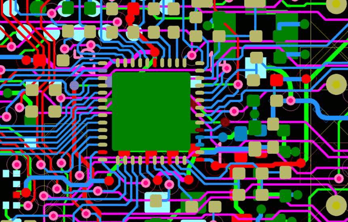
Common Issues And Solutions In PCB Copper Tracing
Printed Circuit Boards (PCBs) are the backbone of modern electronic devices, and copper tracing is a critical component in their design and functionality. However, several common issues can arise in PCB copper tracing, potentially compromising the performance and reliability of the final product. Understanding these issues and their solutions is essential for engineers and designers aiming to produce high-quality PCBs.
One prevalent issue in PCB copper tracing is the occurrence of signal integrity problems.
These problems often manifest as signal loss, noise, or interference, which can degrade the performance of the electronic device. Signal integrity issues are frequently caused by improper trace width, spacing, or routing. To mitigate these problems, designers should adhere to industry standards for trace width and spacing, ensuring that traces are neither too narrow nor too close together. Additionally, employing proper routing techniques, such as avoiding sharp angles and maintaining consistent trace lengths, can significantly enhance signal integrity.
Another common challenge is the occurrence of thermal management issues.
Copper traces can generate significant heat, especially in high-power applications, leading to potential overheating and damage to the PCB and its components. Effective thermal management is crucial to prevent such issues. One solution is to use wider traces for high-current paths, as this reduces resistance and heat generation. Additionally, incorporating thermal vias and heat sinks can help dissipate heat more effectively, ensuring the PCB operates within safe temperature limits.
Corrosion is another issue that can affect PCB copper tracing.
Exposure to moisture, chemicals, and other environmental factors can lead to the oxidation and degradation of copper traces, compromising the PCB’s functionality. To combat corrosion, designers can apply protective coatings, such as solder mask or conformal coating, to shield the copper traces from environmental exposure. Furthermore, selecting high-quality materials and ensuring proper storage conditions can also help minimize the risk of corrosion.
Electromagnetic interference (EMI) is a significant concern in PCB design, particularly in densely packed circuits.
EMI can cause unwanted noise and signal disruption, affecting the performance of the electronic device. To address EMI issues, designers should implement proper grounding techniques, such as using ground planes and ensuring adequate separation between signal and power traces. Additionally, incorporating shielding techniques, such as using metal enclosures or adding ferrite beads, can further reduce EMI and enhance the overall performance of the PCB.
Manufacturing defects can also pose challenges in PCB copper tracing.
Issues such as incomplete etching, over-etching, or misalignment can lead to faulty connections and reduced reliability. To minimize manufacturing defects, it is essential to work with reputable PCB manufacturers who adhere to stringent quality control standards. Additionally, conducting thorough design reviews and simulations before production can help identify and rectify potential issues early in the design process.
In conclusion, while PCB copper tracing is a critical aspect of electronic design, it is not without its challenges. Signal integrity problems, thermal management issues, corrosion, electromagnetic interference, and manufacturing defects are common concerns that can impact the performance and reliability of PCBs. By adhering to industry standards, employing proper design techniques, and working with reputable manufacturers, designers can effectively address these issues and produce high-quality PCBs that meet the demands of modern electronic applications. Through continuous learning and adaptation, the field of PCB design can continue to evolve, ensuring the development of increasingly sophisticated and reliable electronic devices.
Innovations In Copper Clad Laminates For Advanced PCBs
Copper clad laminates (CCLs) are fundamental to the construction of printed circuit boards (PCBs), serving as the substrate upon which electronic components are mounted. Recent innovations in CCLs have significantly advanced the capabilities of PCBs, enabling more complex and efficient electronic devices. These advancements are driven by the increasing demand for higher performance, miniaturization, and reliability in electronic products.
One of the most notable innovations in copper clad laminates is the development of high-frequency laminates.
Traditional CCLs, typically made from materials like FR-4, are not always suitable for high-frequency applications due to their dielectric properties. High-frequency laminates, on the other hand, are designed to minimize signal loss and maintain signal integrity at higher frequencies. These laminates often incorporate materials such as polytetrafluoroethylene (PTFE) and ceramic-filled composites, which offer superior electrical performance. As a result, they are increasingly used in applications such as 5G telecommunications, radar systems, and high-speed data transmission.
In addition to high-frequency laminates, there has been significant progress in the development of high thermal conductivity laminates.
As electronic devices become more powerful, they generate more heat, which can adversely affect performance and reliability. High thermal conductivity laminates are engineered to efficiently dissipate heat, thereby enhancing the thermal management of PCBs. These laminates often utilize materials like metal cores or thermally conductive fillers to achieve their heat-dissipating properties. Consequently, they are particularly valuable in applications such as power electronics, LED lighting, and automotive electronics, where effective thermal management is crucial.
Another area of innovation is the enhancement of the mechanical properties of copper clad laminates.
The trend towards miniaturization and the increasing complexity of electronic devices necessitate laminates that can withstand more rigorous mechanical stresses. Advanced CCLs now incorporate materials that improve their toughness, flexibility, and resistance to environmental factors such as moisture and chemicals. For instance, the use of modified epoxy resins and reinforced glass fabrics has led to laminates that offer better mechanical stability and durability. This makes them suitable for use in harsh environments, such as aerospace and military applications.
Moreover, the push for environmentally friendly electronics has spurred the development of eco-friendly copper clad laminates.
traditional CCLs often contain hazardous substances like brominated flame retardants, which pose environmental and health risks. In response, manufacturers are now producing laminates that are free from such harmful substances, using alternative flame retardants and greener manufacturing processes. These eco-friendly laminates not only comply with stringent environmental regulations but also appeal to consumers and industries that prioritize sustainability.
Furthermore, advancements in manufacturing techniques have also played a crucial role in the evolution of copper clad laminates.
3 Innovations such as laser direct structuring (LDS) and additive manufacturing have enabled more precise and efficient production of CCLs. These techniques allow for the creation of complex circuit patterns and the integration of multiple functionalities into a single laminate. This not only enhances the performance of the final PCB but also reduces production costs and time.
In conclusion, the continuous innovation in copper clad laminates is pivotal to the advancement of printed circuit boards. High-frequency and high thermal conductivity laminates, improved mechanical properties, eco-friendly materials, and advanced manufacturing techniques are all contributing to the development of more capable and reliable PCBs. As the demand for sophisticated electronic devices grows, these innovations will undoubtedly play a critical role in meeting the evolving needs of the industry.