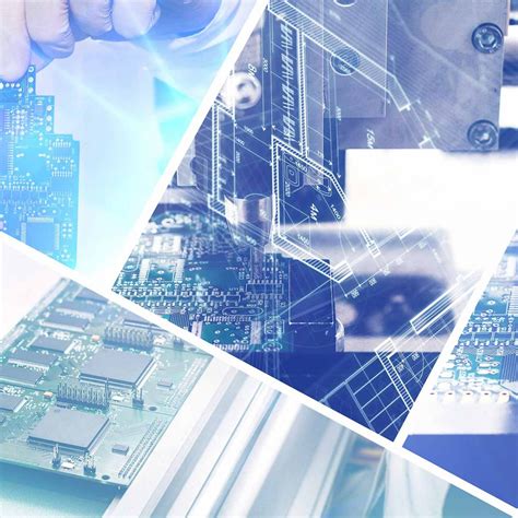
PCB Customization Requirements: A Comprehensive Guide
Introduction
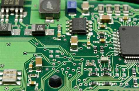
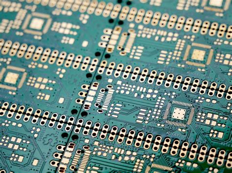
Printed Circuit Boards (PCBs) are the backbone of modern electronic devices, serving as the foundation for electrical connections between components. As technology advances, the demand for customized PCBs has grown significantly. Custom PCBs are tailored to meet specific design, performance, and application requirements, ensuring optimal functionality for various industries, including consumer electronics, automotive, aerospace, and medical devices.
This article explores the key requirements for PCB customization, covering design considerations, material selection, manufacturing constraints, and testing protocols. By understanding these factors, engineers and designers can develop high-performance PCBs that meet exact specifications.
1. Design Requirements for Custom PCBs
The design phase is critical in PCB customization, as it determines the board’s functionality, reliability, and manufacturability. Key design considerations include:
1.1 Schematic Design
- A well-defined schematic diagram is essential for mapping electrical connections.
- Engineers must ensure proper component placement, signal integrity, and power distribution.
- Simulation tools (e.g., SPICE) help verify circuit behavior before fabrication.
1.2 PCB Layout and Routing
- Layer Stackup: Multilayer PCBs (4L, 6L, 8L, etc.) are used for complex circuits, while single/double-layer boards suffice for simpler designs.
- Trace Width and Spacing: Determined by current-carrying capacity and signal integrity requirements.
- High-Speed Design: Controlled impedance routing is necessary for RF and high-frequency applications.
- Thermal Management: Proper heat dissipation through thermal vias and copper pours.
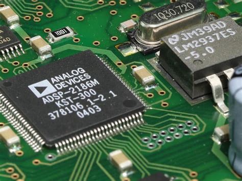
1.3 Component Selection
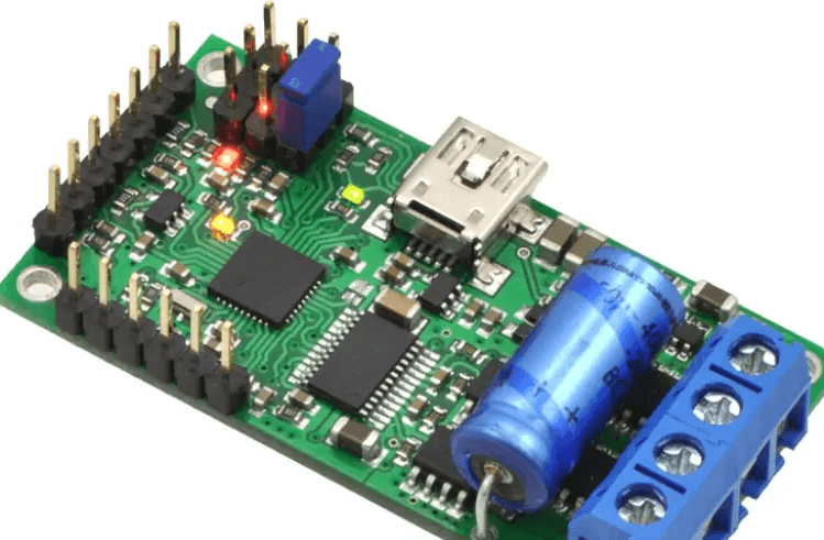
- Through-Hole vs. Surface-Mount (SMT): SMT allows for compact designs, while through-hole offers mechanical strength.
- High-Density Interconnect (HDI): Required for miniaturized PCBs with fine-pitch components.
- BGA and QFN Packages: Need precise soldering techniques.
1.4 Design for Manufacturing (DFM)
- Adhering to manufacturer capabilities (minimum trace width, drill size, etc.).
- Avoiding acid traps, starved thermals, and other manufacturability issues.
- Panelization for efficient assembly.
2. Material Selection for Custom PCBs
The choice of PCB materials impacts performance, durability, and cost. Key materials include:
2.1 Substrate Materials
- FR-4: Standard epoxy laminate, cost-effective for general applications.
- High-Frequency Laminates (Rogers, Teflon): Used in RF/microwave PCBs.
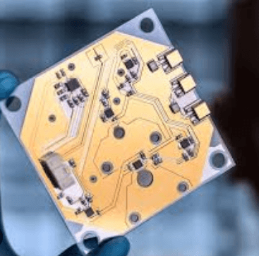
- Flexible PCBs (Polyimide): Suitable for wearable and bendable electronics.
- Metal-Core PCBs (Aluminum, Copper): Enhance heat dissipation in LED and power electronics.
2.2 Copper Thickness
- Standard: 1 oz/ft² (35 µm), but heavy copper (up to 20 oz) is used for high-power applications.
2.3 Surface Finishes
- HASL (Hot Air Solder Leveling): Economical but not ideal for fine-pitch components.
- ENIG (Electroless Nickel Immersion Gold): Provides a flat surface for SMT.
- OSP (Organic Solderability Preservative): Cost-effective but less durable.
- Immersion Silver/Tin: Alternative to ENIG for specific applications.
3. Manufacturing and Assembly Considerations
Custom PCB fabrication involves several critical steps:
3.1 Fabrication Process
- Photolithography: Transferring the circuit pattern onto the board.
- Etching: Removing excess copper to form traces.
- Drilling: Creating vias and through-holes.
- Plating: Electroless or electrolytic copper deposition for conductivity.
- Solder Mask Application: Protects copper traces from oxidation.
- Silkscreen Printing: Component labels and identifiers.
3.2 Assembly Techniques
- SMT Assembly: Automated pick-and-place machines for high-volume production.
- Through-Hole Assembly: Manual or wave soldering for larger components.
- Mixed Assembly: Combining SMT and through-hole components.
3.3 Quality Control
- Automated Optical Inspection (AOI): Detects soldering defects.
- X-Ray Inspection: Essential for BGA and hidden solder joints.
- Electrical Testing: Continuity and functional testing.
4. Testing and Validation
Before deployment, custom PCBs must undergo rigorous testing:
4.1 Electrical Testing
- Continuity Testing: Ensures no open or short circuits.
- In-Circuit Testing (ICT): Validates individual component functionality.
- Functional Testing: Verifies overall board performance under real-world conditions.
4.2 Environmental Testing
- Thermal Cycling: Assesses performance under temperature variations.
- Vibration and Shock Testing: Crucial for automotive and aerospace applications.
- Humidity Testing: Ensures reliability in humid conditions.
4.3 Signal Integrity Testing
- Impedance Matching: Critical for high-speed designs.
- EMI/EMC Testing: Ensures compliance with electromagnetic standards.
5. Industry-Specific Customization Requirements
Different industries have unique PCB requirements:
5.1 Automotive PCBs
- High-temperature resistance.
- Vibration-proof designs.
- Compliance with automotive standards (AEC-Q100).
5.2 Medical PCBs
- Biocompatible materials.
- High reliability for life-critical devices.
- Miniaturization for implantable electronics.
5.3 Aerospace & Defense PCBs
- Radiation-hardened materials.
- Extreme temperature resilience.
- MIL-STD and IPC Class 3 compliance.
5.4 Consumer Electronics
- Cost-effective manufacturing.
- Compact and lightweight designs.
- High-speed signal integrity.
6. Future Trends in PCB Customization
- 3D-Printed PCBs: Rapid prototyping with additive manufacturing.
- Embedded Components: Integrating passive components within the PCB layers.
- AI-Driven Design Optimization: Automated layout and routing for efficiency.
- Sustainable Materials: Eco-friendly substrates and lead-free soldering.
Conclusion
Custom PCB design requires careful consideration of electrical, mechanical, and environmental factors. By optimizing design, material selection, manufacturing processes, and testing protocols, engineers can develop high-performance PCBs tailored to specific applications. As technology evolves, PCB customization will continue to play a pivotal role in advancing electronics across industries.
By adhering to these requirements, businesses can ensure reliability, efficiency, and innovation in their electronic products. Whether for consumer gadgets, medical devices, or aerospace systems, customized PCBs are the key to next-generation electronic solutions.