PCB Design Basics: A Comprehensive Guide for Beginners
Introduction to PCB Design
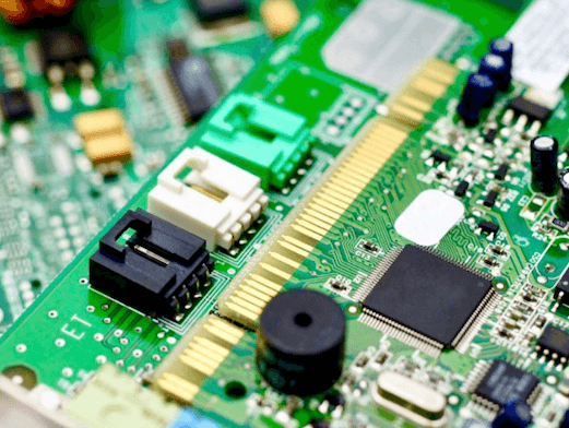
Printed Circuit Board (PCB) design is a fundamental aspect of modern electronics. PCBs serve as the backbone of electronic devices, providing mechanical support and electrical connections between components. Whether you’re designing a simple LED circuit or a complex motherboard, understanding PCB design basics is essential for creating reliable and efficient electronic products.
This guide covers the fundamental concepts of PCB design, including schematic creation, component placement, routing, and manufacturing considerations.
1. Understanding PCB Layers and Materials
1.1 PCB Layers
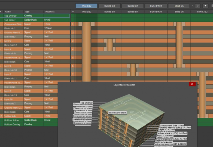
PCBs can be single-sided, double-sided, or multi-layered:
- Single-layer PCBs: Conducting material (usually copper) on one side only, suitable for simple circuits.
- Double-layer PCBs: Copper on both sides, allowing more complex routing.
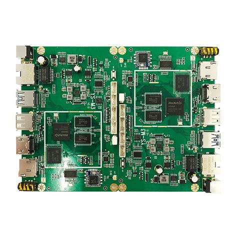
- Multi-layer PCBs: Used in high-density designs (e.g., smartphones, computers) with internal signal and power planes.
1.2 PCB Materials
The most common substrate material is FR-4, a flame-resistant fiberglass epoxy laminate. Other materials include:
- Flexible PCBs (Polyimide): Used in wearable electronics.
- High-frequency materials (Rogers, Teflon): For RF and microwave applications.
- Metal-core PCBs: For high-power applications (e.g., LED lighting).
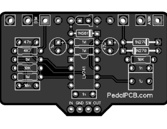
2. Schematic Design: The Foundation of PCB Layout
Before designing the PCB, you need a schematic diagram, which represents the electrical connections between components.
2.1 Key Steps in Schematic Design
- Component Selection: Choose resistors, capacitors, ICs, and connectors.
- Symbol Placement: Place symbols representing each component.
- Net Connections: Draw wires (nets) to define electrical connections.
- Annotation & BOM: Label components and generate a Bill of Materials (BOM).
2.2 Best Practices for Schematic Design
- Use clear and consistent naming for components and nets.
- Group related circuits (e.g., power supply, microcontroller section).
- Add notes and labels for readability.
- Verify connections using Electrical Rule Check (ERC).
3. PCB Layout: From Schematic to Physical Design
Once the schematic is ready, the next step is PCB layout, where components are placed and routed on the board.
3.1 PCB Design Workflow
- Import Netlist: Transfer connections from the schematic to the PCB editor.
- Define Board Shape & Layers: Set dimensions and layer stack-up.
- Component Placement: Position components logically.
- Routing: Connect components with copper traces.
- Design Rule Check (DRC): Ensure manufacturability.
- Generate Gerber Files: For PCB fabrication.
3.2 Component Placement Strategies
- Functional Grouping: Place related components (e.g., microcontroller and its peripherals) together.
- Signal Flow: Arrange components to minimize trace lengths (e.g., shortest path for high-speed signals).
- Thermal Considerations: Keep heat-generating components (e.g., voltage regulators) away from sensitive parts.
- Mechanical Constraints: Consider enclosure size and mounting holes.
3.3 Routing Techniques
- Trace Width & Current Capacity: Wider traces handle higher currents (use a trace width calculator).
- Signal Integrity: Avoid sharp angles (use 45° or curved traces).
- Ground & Power Planes: Use solid copper pours for better EMI performance.
- Differential Pairs: Route high-speed signals (USB, HDMI) as tightly coupled pairs.
4. Design Rules and Manufacturing Considerations
4.1 Design Rules Checklist
- Minimum Trace Width & Spacing: Typically 6-10 mils (0.15-0.25 mm) for standard PCBs.
- Via Sizes: Through-hole vias (0.3-0.5 mm), microvias for HDI designs.
- Clearance Rules: Ensure no short circuits between traces/pads.
- Solder Mask & Silkscreen: Define openings for soldering and component labels.
4.2 Avoiding Common PCB Design Mistakes
- Insufficient Power Distribution: Use proper decoupling capacitors.
- Poor Grounding: Avoid ground loops; use a solid ground plane.
- Incorrect Footprints: Verify component dimensions before placement.
- Ignoring Thermal Management: Add thermal vias for heat dissipation.
5. PCB Fabrication and Assembly
5.1 PCB Fabrication Process
- Gerber File Generation: Export manufacturing files (copper layers, solder mask, silkscreen).
- Drilling: Holes for vias and through-hole components.
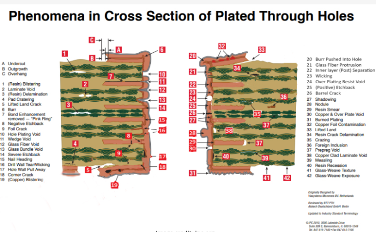
- Plating & Etching: Copper deposition and unwanted copper removal.
- Solder Mask Application: Insulating layer to prevent shorts.
- Silkscreen Printing: Component labels and logos.
- Surface Finish: HASL, ENIG, or OSP for solderability.
5.2 PCB Assembly (PCBA)
- Through-Hole (THT): Components inserted into drilled holes.
- Surface-Mount (SMT): Components soldered directly onto pads.
- Testing & Inspection: Verify functionality (e.g., flying probe, AOI).
6. Advanced PCB Design Considerations
6.1 High-Speed Design
- Impedance Control: Match trace impedance for RF/high-speed signals.
- Signal Integrity: Minimize crosstalk with proper spacing.
- EMI/EMC Compliance: Use shielding and proper grounding.
6.2 Mixed-Signal Design
- Separate analog and digital grounds to avoid noise coupling.
- Use star grounding for sensitive circuits.
6.3 Design for Manufacturing (DFM)
- Follow manufacturer’s guidelines for minimum tolerances.
- Avoid acid traps (acute angles in traces).
- Ensure proper copper balancing to prevent warping.
7. PCB Design Tools
Popular PCB design software includes:
- KiCad (Free & Open-Source)
- Altium Designer (Professional)
- Eagle (Autodesk)
- OrCAD (Cadence)
- Proteus (Labcenter Electronics)
Conclusion
PCB design is a blend of art and engineering, requiring attention to detail, electrical knowledge, and manufacturing awareness. By mastering the basics—schematic design, component placement, routing, and DFM—you can create reliable and efficient PCBs for any application.
Whether you’re a hobbyist or a professional, continuous learning and practice will enhance your PCB design skills. Start with simple projects, experiment with different techniques, and gradually tackle more complex designs.
Further Reading & Resources
- IPC Standards (PCB Manufacturing Guidelines)
- “High-Speed Digital Design” by Howard Johnson
- Online PCB Design Courses (Udemy, Coursera)