PCB Design Considerations: Key Points for Successful Circuit Board Layout
Introduction
Printed Circuit Board (PCB) design is a crucial step in electronic product development. A well-designed PCB ensures proper functionality, reliability, and manufacturability. However, poor design choices can lead to signal integrity issues, electromagnetic interference (EMI), thermal problems, and manufacturing defects. This article outlines essential considerations for PCB design to help engineers and hobbyists create high-quality circuit boards.
1. Schematic Design and Preparation
Before starting PCB layout, a well-structured schematic is necessary.
1.1 Component Selection
- Choose components based on availability, cost, and performance.
- Verify footprint compatibility between the schematic symbol and PCB layout.
- Consider alternative parts in case of supply chain shortages.
1.2 Netlist and Design Rules
- Ensure all connections are correctly defined in the schematic.
- Define design rules early (trace width, clearance, via sizes) to avoid errors later.

2. PCB Layout Best Practices
2.1 Board Stackup and Layer Planning
- Single-layer PCBs: Suitable for simple circuits but limited in routing flexibility.
- Double-layer PCBs: More routing options, better for moderate complexity.
- Multilayer PCBs (4+ layers): Essential for high-speed designs, providing dedicated power and ground planes.
Key Tips:
- Place ground and power planes adjacent to minimize impedance.
- Use symmetrical stackups to prevent warping during manufacturing.
2.2 Component Placement
- Group related components (e.g., power supply, analog, digital sections).
- Place critical components first (MCUs, connectors, high-speed ICs).
- Consider thermal management: Position heat-generating parts near ventilation or heatsinks.
- Minimize trace lengths between connected components to reduce noise.
2.3 Routing Considerations
Signal Integrity
- Avoid sharp angles (use 45° or curved traces to reduce reflections).
- Match trace lengths for differential pairs (e.g., USB, Ethernet).
- Control impedance for high-speed signals (consult manufacturer guidelines).
Power and Ground Routing
- Use wide traces for power lines to minimize voltage drop.
- Implement a solid ground plane to reduce noise and EMI.
- Avoid ground loops by ensuring a low-impedance return path.
Avoiding Crosstalk
- Separate high-speed and sensitive analog traces.
- Increase spacing between parallel traces to reduce coupling.
- Use ground shielding between critical signals if necessary.
2.4 Via Usage
- Minimize via count in high-speed paths to reduce inductance.
- Use stitching vias to connect ground planes in multilayer designs.
- Avoid placing vias under BGA pads to prevent soldering issues.
2.5 Thermal Management
- Use thermal relief pads for easier soldering of ground/power connections.
- Add copper pours to dissipate heat from high-power components.
- Consider thermal vias to transfer heat to inner layers or the opposite side.
2.6 Design for Manufacturing (DFM)
- Follow the manufacturer’s design rules (minimum trace width, hole sizes, etc.).
- Ensure proper solder mask and silkscreen clearance to avoid assembly issues.
- Include fiducial marks for automated PCB assembly (pick-and-place machines).
2.7 Design for Testing (DFT)
- Add test points for critical signals to facilitate debugging.
- Ensure probe accessibility for in-circuit testing (ICT).
- Consider boundary scan (JTAG) for complex digital boards.
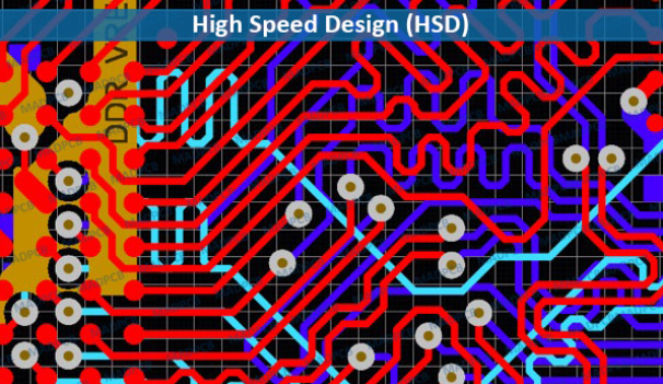
3. High-Speed Design Considerations
High-speed PCBs (e.g., DDR memory, RF circuits) require extra attention:
3.1 Controlled Impedance Routing
- Calculate trace width and spacing based on dielectric material (e.g., FR4, Rogers).
- Use microstrip or stripline configurations for consistent impedance.
3.2 Signal Termination
- Apply series termination (resistors) to reduce reflections.
- Use parallel termination for transmission line matching.
3.3 EMI Mitigation
- Keep high-frequency traces away from board edges.
- Use guard traces or ground shielding for sensitive signals.
- Add ferrite beads or filters to suppress noise.
4. Final Checks Before Manufacturing
4.1 Design Rule Check (DRC)
- Run DRC to detect spacing violations, unconnected nets, and other errors.
4.2 Electrical Rule Check (ERC)
- Verify no floating pins, incorrect power connections, or short circuits.
4.3 Gerber File Verification
- Review Gerber files in a viewer (e.g., KiCad GerbView, online tools).
- Confirm layer alignment, drill holes, and solder mask openings.
4.4 Prototyping and Testing
- Order a small batch first to validate the design.
- Perform functional testing, signal integrity checks, and thermal analysis.
Conclusion
PCB design is a balance of electrical performance, manufacturability, and cost. By following these guidelines—proper schematic preparation, strategic component placement, careful routing, and thorough verification—you can avoid common pitfalls and produce reliable circuit boards. Whether designing simple hobbyist projects or complex industrial systems, adhering to best practices ensures a successful PCB layout.
Would you like additional details on any specific aspect, such as high-speed routing or EMI reduction techniques?