PCB design experience
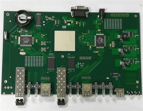
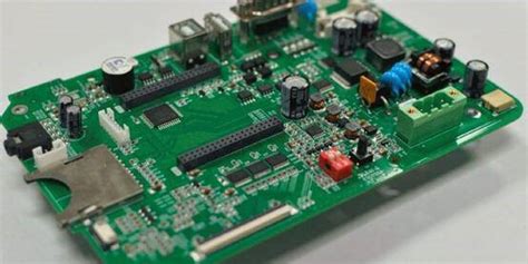
When it comes to PCB boards, many friends will think of it everywhere around us, from all household appliances, various accessories in computers, to various digital products. Almost all electronic products will use PCB boards, so what exactly is a PCB board? PCB board is Printed Circuit Block, that is, a printed circuit board for electronic components to be inserted and a base with circuits. The copper-plated base is printed with anti-corrosion circuits by printing, and then etched and flushed out.
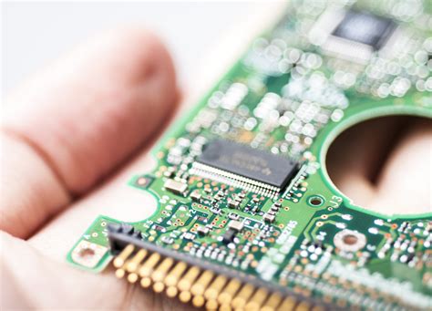
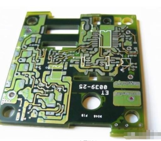
PCB boards can be divided into single-layer boards, double-layer boards and multi-layer boards. Various electronic components are integrated on PCB boards. On the most basic single-layer PCB, the parts are concentrated on one side and the wires are concentrated on the other side. In this way, we need to make holes in the board so that the pins can pass through the board to the other side, so the pins of the parts are soldered on the other side. Because of this, the front and back sides of such PCBs are called component side and solder side respectively.
Double-layer boards can be seen as two single-layer boards bonded together, with electronic components and traces
on both sides of the board. Sometimes it is necessary to connect a single line on one side to the other side of the board, which requires a via. A via is a small hole filled or coated with metal on the PCB, which can be connected to the wires on both sides. Now many computer motherboards are using 4-layer or even 6-layer PCBs, while graphics cards generally use 6-layer PCBs. Many high-end graphics cards like the nVIDIAGeForce4Ti series use 8-layer PCBs, which are so-called multi-layer PCBs.
On multi-layer PCBs, there will also be problems connecting the lines between layers, which can also be achieved through vias.
Because it is a multi-layer PCB, sometimes the via does not need to penetrate the entire PCB. Such vias are called buried vias and blind vias because they only penetrate a few layers. Blind vias connect several layers of internal PCB to the surface PCB without penetrating the entire board. Buried vias only connect the internal PCB, so they cannot be seen from the surface. In a multilayer PCB, the entire layer is directly connected to the ground and power supply. So we classify each layer as a signal layer, a power layer, or a ground layer. If the parts on the PCB require different power supplies, this type of PCB usually has more than two layers of power and wire layers. The more layers of PCB boards used, the higher the cost. Of course, using more layers of PCB boards is very helpful in providing signal stability.
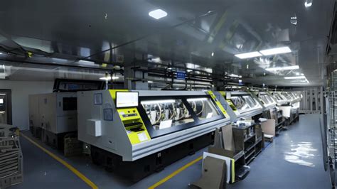
The product
ion process of professional PCB boards is quite complicated. Take a 4-layer PCB board as an example. The PCB of the motherboard is mostly 4 layers. During manufacturing, the middle two layers are first rolled, cut, etched, and oxidized and electroplated. These 4 layers are the component surface, power layer, ground layer, and solder layer. Then put these 4 layers together and roll them into a PCB for the motherboard. Then punch and make holes. After cleaning, print the circuits of the outer two layers, apply copper, etch, test, solder mask, and silk screen.
Finally, the entire PCB (including many motherboards) is punched into motherboard PCBs, and then vacuum-packed after passing the test.
If the copper foil is not applied well during the PCB production process, there will be a phenomenon of loose adhesion, which is easy to imply short circuits or capacitance effects (easy to cause interference). The vias on the PCB must also be paid attention to. If the hole is not punched in the middle, but biased to one side, it will produce uneven matching, or it is easy to contact the power layer or ground layer in the middle, resulting in potential short circuits or poor grounding factors.
Copper wire wiring process
The first step in production is to establish the wiring between parts. We use negative film transfer to show the working film on the metal conductor. This technique is to cover the entire surface with a thin layer of copper foil and eliminate the excess part. Additional transfer is another less used method. This is a method of applying copper wire only where it is needed, but we will not talk about it here. Positive photoresist is made of photosensitive agent, which will dissolve under lighting. There are many ways to treat photoresist on copper surfaces, but the most common way is to heat it and roll it over the surface containing photoresist.
It can also be sprayed on in liquid form, but dry film provides higher resolution and can also produce thinner wires.
The light shield is just a template for the PCB layer in manufacturing. Before the photoresist on the PCB board is exposed to UV light, the light shield covering it can prevent the photoresist in some areas from being exposed. These areas covered by the photoresist will become wiring. After the photoresist is developed, the other bare copper parts are etched. The etching process can be done by immersing the board in an etching solvent or spraying the solvent on the board. Ferric chloride is generally used as an etching solvent. After etching, the remaining photoresist is removed.
- Wiring width and current
Generally, the width should not be less than 0.2mm (8mil)
On high-density and high-precision PCBs, the spacing and line width are generally 0.3mm (12mil).
When the thickness of the copper foil is about 50um, the wire width is 1~1.5mm (60mil) = 2A
The common ground is generally 80mil, and it is more important for applications with microprocessors.
2.How high a frequency is considered a high-speed board?
When the rising/falling edge time of the signal is 3~6 times the signal transmission time, it is considered a high-speed signal.
For digital circuits, the key is to look at the steepness of the edge of the signal, that is, the rise and fall time of the signal.
According to the theory of a very classic book “High Speed Digital Design”, the time for the signal to rise from 10% to 90% is less than 6 times the wire delay, which is a high-speed signal!——That is! Even if it is an 8KHz square wave signal, as long as the edge is steep enough, it is also a high-speed signal, and the transmission line theory needs to be used when wiring.
3.Stacking and layering of PCB boards
There are several stacking orders for four-layer boards. The following are the advantages and disadvantages of various stacking layers:
First case
GND
S1+POWER
S2+POWER
GND
Second case
SIG1
GND
POWER
SIG2
Third case
GND
S1
S2
POWER
Note: S1 is the first layer of signal wiring, S2 is the second layer of signal wiring; GND ground layer POWER power layer
The first case should be the best case among the four-layer boards. Because the outer layer is the ground layer, it has a shielding effect on EMI, and the power layer and the ground layer are also very close, so that the internal resistance of the power supply is small and the best effect is achieved. However, the first case cannot be used when the density of the board is relatively high. Because in this way, the integrity of the first layer of ground cannot be guaranteed, so the signal of the second layer will become worse. In addition, this structure cannot be used when the power consumption of the whole board is relatively high.
The second case is the most commonly used method.
From the structure of the board, it is not suitable for high-speed digital circuit design. Because in this structure, it is not easy to maintain low power supply impedance. Take a 2mm board as an example: Z0=50ohm is required. The line width is 8mil. The copper foil thickness is 35цm. In this way, the distance between the signal layer and the ground layer is 0.14mm. The distance between the ground layer and the power layer is 1.58mm. This greatly increases the internal resistance of the power supply. In this structure, since the radiation is toward space, a shielding plate is required to reduce EMI.
In the third case, the signal line quality on the S1 layer is the best. S2 is second. It has a shielding effect on EMI. But the power supply impedance is large. This board can be used when the power consumption of the whole board is large and the board is the interference source or is close to the interference source.
4.Impedance matching
The amplitude of the reflected voltage signal is determined by the source reflection coefficient ρs and the load reflection coefficient ρL
ρL = (RL – Z0) / (RL + Z0) and ρS = (RS – Z0) / (RS + Z0)
In the above formula, if RL = Z0, the load reflection coefficient ρL = 0. If RS = Z0, the source reflection coefficient ρS = 0.
Since the ordinary transmission line impedance Z0 should usually meet the requirement of 50Ω, and the load impedance is usually in the thousands of ohms to tens of thousands of ohms.
Therefore, it is difficult to achieve impedance matching at the load end. However, since the signal source end (output) impedance is usually relatively small, roughly a dozen ohms. Therefore, it is much easier to achieve impedance matching at the source end. If a resistor is connected in parallel at the load end, the resistor will absorb part of the signal and is not conducive to transmission (my understanding). When the TTL/CMOS standard 24mA drive current is selected, its output impedance is approximately 13Ω. If the transmission line impedance Z0 = 50Ω, then a 33Ω source end matching resistor should be added. 13Ω+33Ω=46Ω (approximately 50Ω, weak underdamping helps the setup time of the signal)
When choosing other transmission standards and driving currents, the matching impedance will be different. In high-speed logic and circuit design, for some key signals, such as clocks, control signals, etc., we recommend adding source matching resistors.
In this way, the signal will be reflected back from the load end, because the source impedance is matched, and the reflected signal will not be reflected back again.

5.Precautions for power line and ground line layout
The power line should be as short as possible, in a straight line, and it is best to go in a tree shape instead of a ring shape
Ground loop problem: For digital circuits, the ground loop current caused by the ground loop is only at the level of tens of millivolts, while the anti-interference threshold of TTL is 1.2V, and the CMOS circuit can reach 1/2 of the power supply voltage, which means that the ground loop current will not have any adverse effect on the operation of the circuit.
On the contrary, if the ground wire is not closed, the problem will be even greater
because the pulse power supply current generated by the digital circuit when working will cause the ground potential of each point to be unbalanced. For example, I measured that the ground current of 74LS161 was 1.2A when it was reversed (measured by a 2Gsps oscilloscope, the ground current pulse width was 7ns). Under the impact of large pulse current, if a branch ground wire (line width 25mil) is used, the potential difference between each point between the ground wires will reach the level of hundreds of millivolts.
After the ground wire loop is used, the pulse current will be spread to each point of the ground wire, greatly reducing the possibility of interfering with the circuit. With a closed ground wire, the maximum instantaneous potential difference of the ground wire of each device is measured to be one-half to one-fifth of that of an unclosed ground wire.
Of course, the measured data of circuit boards with different densities and speeds vary greatly. What I said above refers to the level of the Z80 Demo board attached to Protel 99SE; for low-frequency analog circuits, I think the power frequency interference after the ground wire is closed is sensed from space, which cannot be simulated or calculated in any way. If the ground wire is not closed, no ground wire eddy current will be generated.
What is the theoretical basis of Beckhamtao’s so-called “but the power frequency induced voltage will be greater if the ground wire is open-loop?”? Let me give you two examples. Seven years ago, I took over a project from someone else, a precision pressure gauge, which used a 14-bit A/D converter, but the actual measurement showed only 11-bit effective accuracy. After investigation, it was found that there was 15mVp-p power frequency interference on the ground wire. The solution was to cut the analog ground loop of the PCB, and use flying wires to make branch-like distribution of the ground wire from the front-end sensor to the A/D. Later, the mass-produced model PCB was re-produced according to the routing of the flying wire, and no problems have occurred so far. The second example is that a friend loves fever and DIYed an amplifier by himself, but there is always AC sound in the output. I suggested that he cut the ground loop and the problem was solved. Afterwards, this guy checked dozens of “Hi-Fi famous machine” PCB diagrams and confirmed that no machine uses a ground loop in the analog part.
6.PCB design principles and anti-interference measures
PCB is the support for circuit elements and devices in electronic products. It provides electrical connections between circuit elements and devices. With the rapid development of electronic technology, the density of PCB is getting higher and higher. The quality of PCB design has a great impact on the anti-interference ability. Therefore, when designing PCB, the general principles of PCB design must be followed and the requirements of anti-interference design must be met.
General principles of PCB design
To achieve the best performance of electronic circuits, the layout of components and wires is very important. In order to design a PCB with good quality and low cost, the following general principles should be followed:
Layout
First, consider the size of the PCB. When the PCB size is too large, the printed lines are long, the impedance increases, the anti-noise ability decreases, and the cost increases; if it is too small, the heat dissipation is not good, and the adjacent lines are susceptible to interference. After determining the PCB size, determine the location of special components. Finally, layout all components of the circuit according to the functional units of the circuit.
The following principles should be followed when determining the location of special components:
(1) Keep the connections between high-frequency components as short as possible, and try to reduce their distributed parameters and mutual electromagnetic interference. Components susceptible to interference should not be placed too close to each other, and input and output components should be kept as far away as possible.
(2) There may be a high potential difference between some components or wires, and the distance between them should be increased to avoid discharge leading to accidental short circuits. Components with high voltage should be placed in places that are difficult to reach during debugging.
(3) Components weighing more than 15g should be fixed with a bracket and then soldered. Components that are large, heavy, and generate a lot of heat should not be installed on printed circuit boards, but should be installed on the chassis bottom plate of the whole machine, and heat dissipation should be considered. Thermistors should be kept away from heating components.
(4) The layout of adjustable components such as potentiometers, adjustable inductors, variable capacitors, and micro switches should take into account the structural requirements of the whole machine. If it is adjusted inside the machine, it should be placed in a convenient place on the printed circuit board for adjustment; if it is adjusted outside the machine, its position should be consistent with the position of the adjustment knob on the chassis panel.
(5) The space occupied by the printed plate positioning hole and the fixing bracket should be reserved.
According to the functional units of the circuit, when laying out all the components of the circuit, the following principles should be followed:
(1) Arrange the positions of each functional circuit unit according to the flow of the circuit, so that the layout is convenient for signal flow and the signal can maintain the same direction as much as possible.
(2) Take the core component of each functional circuit as the center and lay it out around it. Components should be arranged evenly, neatly and compactly on the PCB. Minimize and shorten the leads and connections between components.
(3) For circuits working at high frequencies, the distribution parameters between components should be considered. In general, components should be arranged in parallel as much as possible in circuits. This is not only beautiful, but also easy to assemble and solder, and easy to mass produce.
(4) Components located at the edge of the circuit board are generally not less than 2mm away from the edge of the circuit board. The best shape of the circuit board is a rectangle. The aspect ratio is 3:2 to 4:3. When the size of the circuit board is larger than 200x150mm, the mechanical strength of the circuit board should be considered.
2.Wiring
The wiring principles are as follows:
(1) The wires used for input and output terminals should be avoided to be parallel to each other. It is best to add a ground wire between the wires to avoid feedback coupling.
(2) The minimum width of the printed wiring is mainly determined by the adhesion strength between the wire and the insulating substrate and the current flowing through them.