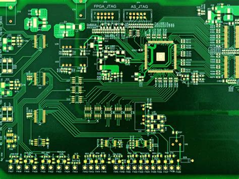
PCB Design & Fabrication: Enhancing Efficiency and Reliability

Key Takeaways
Effective PCB design & fabrication relies on balancing efficiency and reliability across all stages. Central to this is adopting optimized layout practices, such as minimizing trace lengths and ensuring proper thermal management, which reduces signal interference and improves performance. Material selection plays a pivotal role—choosing substrates with high glass transition temperatures (Tg) or low-loss dielectrics enhances durability in demanding environments.
"Integrating Design for Manufacturability (DFM) checks early in the design phase prevents costly revisions during PCB assembly."
Advanced fabrication techniques, including laser drilling and automated optical inspection (AOI), elevate precision while reducing defects. For PCBA workflows, combining surface-mount technology (SMT) with rigorous testing protocols ensures consistent quality. Below is a comparison of traditional vs. advanced approaches:
| Factor | Traditional Methods | Advanced Techniques |
|---|---|---|
| Accuracy | ±50 μm tolerances | ±10 μm laser-guided drilling |
| Inspection | Manual visual checks | AOI with AI-driven defect detection |
| Throughput | 50-100 boards/day | 200+ boards/day with automation |
To reduce costs without compromising reliability, consider panelization to maximize material use and streamline PCB assembly. Prioritize collaboration between design and fabrication teams to align electrical requirements with manufacturing capabilities. Finally, leverage simulation tools to validate signal integrity and power distribution before moving to production.
Streamlining PCB Design Process Optimization
Effective PCB design optimization begins with systematic planning of component placement and routing strategies. Utilizing advanced CAD tools enables engineers to visualize signal integrity challenges early, reducing iterative revisions during pcb assembly. Implementing Design for Manufacturability (DFM) principles ensures compatibility with automated pcba workflows, minimizing alignment errors in high-volume production.
Critical to this process is the integration of modular design frameworks, which standardize reusable circuit blocks for faster prototyping. For instance, grouping power regulation components separately from analog signal paths simplifies testing and pcb fabrication adjustments. Additionally, adopting automated design rule checks (DRC) accelerates error detection, particularly for trace spacing and via placement—key factors affecting pcba reliability.
Transitioning to cloud-based collaboration platforms further streamlines workflows, allowing real-time feedback between design and fabrication teams. By prioritizing thermal management in layout planning—such as optimizing copper pours for heat dissipation—engineers enhance long-term performance across pcb assembly stages. This holistic approach not shortens development cycles but ensures seamless alignment with downstream manufacturing requirements.
Efficient PCB Layout Design Best Practices
Effective PCB design begins with optimizing component placement to minimize signal path lengths and reduce electromagnetic interference. Prioritize critical traces—such as clock lines and high-speed signals—by routing them first, using differential pairs where applicable to enhance noise immunity. Maintain consistent trace widths for power and ground planes to ensure uniform current distribution, while avoiding sharp angles to prevent impedance discontinuities.
Integrating design for manufacturability (DFM) principles early reduces errors during PCB assembly. For instance, aligning component orientations simplifies automated PCBA processes, improving placement accuracy. Utilize thermal relief pads for through-hole components to balance heat dissipation and solderability, particularly in mixed-technology boards.
Leverage advanced simulation tools to validate signal integrity and power delivery networks before fabrication. Implementing grid-based routing and adhering to industry-standard clearance rules (e.g., IPC-2221) ensures compatibility with high-precision PCB fabrication equipment. Finally, collaborate closely with PCBA partners to align layout choices with their capabilities, reducing rework and accelerating time-to-market.
Material Selection Strategies for Reliable PCBs
Effective PCB design & fabrication hinges on strategic material choices that balance electrical performance, thermal management, and mechanical durability. Selecting the right substrate materials, such as high-temperature FR-4 or specialized laminates like polyimide, directly impacts signal integrity and resistance to environmental stressors. For high-frequency applications, low-loss dielectrics (e.g., Rogers RO4000 series) minimize signal attenuation, while thermally conductive materials enhance heat dissipation in power-dense designs.
In PCB assembly (PCBA), compatibility between base materials and soldering processes is critical. For instance, choosing copper weights aligned with current-carrying requirements ensures reliable traces, while surface finishes like ENIG (Electroless Nickel Immersion Gold) or HASL (Hot Air Solder Leveling) optimize solderability and corrosion resistance. Additionally, thermal expansion coefficients (CTE) must match between layers to prevent delamination during temperature cycling.
Material selection also influences fabrication efficiency. Opting for standardized substrates reduces lead times, whereas advanced materials like halogen-free laminates meet regulatory standards without compromising performance. By integrating these strategies, engineers can mitigate risks in PCBA workflows and achieve repeatable outcomes in complex electronic systems, laying a foundation for discussing advanced manufacturing techniques in subsequent sections.
Advanced Techniques in PCB Fabrication Efficiency
Modern fabrication facilities leverage automated optical inspection (AOI) systems to detect microscopic defects in PCB assembly processes, reducing human error by over 40%. The adoption of laser direct imaging (LDI) technology eliminates photomasks, enabling faster prototyping and tighter tolerances for high-density interconnects. To optimize material usage, manufacturers now employ dynamic panelization algorithms that nest multiple designs into single panels, minimizing waste while maintaining PCBA yield rates.
Advanced plasma etching techniques ensure precise copper removal for ultra-fine traces, critical for high-frequency applications. Additionally, real-time process monitoring integrates IoT sensors to track parameters like temperature and humidity, automatically adjusting equipment settings to maintain consistency. For multilayer boards, sequential lamination methods reduce warpage risks by controlling thermal stress during layer bonding.
The shift toward modular fabrication lines allows rapid reconfiguration between PCB assembly batches, cutting downtime by 30% while supporting mixed-volume production. By combining these innovations with PCBA-specific design-for-manufacturing (DFM) checks, engineers achieve a 25% improvement in fabrication cycle times without compromising reliability. Transitioning to such techniques ensures seamless alignment with evolving industry demands for speed and precision.
Ensuring PCB Manufacturing Reliability Standards
Maintaining rigorous reliability standards in PCB manufacturing requires a multi-layered approach that integrates design validation, material consistency, and process control. Thermal cycling tests and electrical stress simulations are critical for identifying potential failures in pcb assembly under real-world operating conditions. For instance, using high-grade substrates and specialized laminates minimizes delamination risks, while precise solder mask application prevents short circuits during pcba production.
Advanced inspection tools, such as automated optical inspection (AOI) systems, ensure dimensional accuracy and trace integrity, reducing defects in high-density interconnect (HDI) designs. Equally critical is adherence to industry certifications like IPC-A-600 and IPC-6012, which define acceptance criteria for surface finishes and plated through-holes. By coupling these protocols with statistical process control (SPC), manufacturers can monitor variables such as etch rates and copper thickness in real time, ensuring consistent output.
Environmental factors, including humidity and chemical contaminants, further challenge reliability. Implementing nitrogen-filled reflow ovens and conformal coatings mitigates oxidation and moisture ingress, extending the lifespan of pcb assembly components. Additionally, collaboration between design and fabrication teams enables proactive adjustments—such as optimizing pad sizes for pcba soldering—to align with manufacturing capabilities. By integrating Design for Manufacturing (DFM) principles early, engineers balance performance demands with producibility, achieving repeatable quality across batches.
Automation in PCB Production: Speed & Precision
The integration of automation in PCB assembly processes has revolutionized manufacturing workflows, delivering unprecedented speed and precision while minimizing human error. Advanced robotic systems now handle tasks such as solder paste application, component placement, and PCBA testing, achieving tolerances as tight as ±0.025mm. These systems leverage machine vision and real-time feedback loops to ensure alignment accuracy, even for high-density designs with micro-BGA or 0201 components.
Process optimization extends beyond hardware—AI-driven software tools analyze production data to predict bottlenecks and adjust parameters dynamically. For instance, automated optical inspection (AOI) systems scan boards at 3D resolutions, flagging defects like solder bridging or misaligned parts before they escalate. This predictive maintenance approach reduces rework rates by up to 40%, directly enhancing PCB fabrication reliability.
Moreover, automated workflows streamline transitions between PCB design and manufacturing phases. Design-for-manufacturability (DFM) checks are now embedded in CAD tools, automatically flagging potential issues like insufficient copper clearance or thermal imbalances. By synchronizing PCBA processes with design intent, manufacturers achieve faster turnaround times without compromising quality—a critical advantage in industries demanding rapid prototyping or mass production scalability.
As automation evolves, its role in balancing cost-efficiency with technical rigor remains central to advancing modern electronics manufacturing.
Cost-Effective PCB Design & Fabrication Methods
Achieving cost efficiency in PCB design & fabrication requires balancing technical precision with budget constraints. A foundational strategy involves optimizing design for manufacturability (DFM) principles, which minimize material waste and reduce rework during PCB assembly. By leveraging standardized component footprints and avoiding overly complex layouts, designers can streamline both prototyping and mass production phases. For instance, selecting widely available substrates like FR-4 instead of specialized materials lowers costs without compromising reliability in most applications.
Integrating PCBA (printed circuit board assembly) automation further enhances affordability. Automated pick-and-place systems and solder paste inspection tools reduce human error, accelerating production while maintaining consistency. To cut expenses, consider partnering with fabrication houses that offer bulk pricing for high-volume orders or shared panelization services. Additionally, adopting modular design practices allows reuse of validated circuit blocks across projects, reducing development time and testing costs.
Material selection also plays a pivotal role. Using surface finishes like HASL (Hot Air Solder Leveling) instead of premium options like ENIG (Electroless Nickel Immersion Gold) can yield significant savings for non-critical applications. However, ensure compatibility with PCB assembly processes to avoid hidden costs from compatibility issues. Finally, implementing rigorous design rule checks (DRC) early in the workflow prevents costly revisions post-fabrication, aligning with both efficiency and reliability goals.
Conclusion
The journey from PCB design to fabrication underscores the critical balance between efficiency and reliability in modern electronics. By integrating optimized layout principles with advanced pcb assembly techniques, engineers can mitigate risks such as signal interference or thermal stress, ensuring robust performance in end-use environments. The adoption of PCBA (Printed Circuit Board Assembly) automation not only accelerates production timelines but also enhances precision, reducing human error in component placement and soldering. Furthermore, selecting materials with high thermal stability and low dielectric loss directly impacts long-term durability, particularly in applications demanding extreme operational conditions.
To maintain competitiveness, manufacturers must prioritize collaborative workflows between design and fabrication teams, leveraging tools like Design for Manufacturability (DFM) checks to preempt costly revisions. Innovations in pcb fabrication, such as laser drilling and controlled impedance routing, further refine product quality while adhering to stringent industry standards. Ultimately, achieving cost-effective outcomes without compromising reliability hinges on a holistic approach—one that harmonizes cutting-edge technologies with proven methodologies across both PCB design and assembly stages. This iterative process ensures that every phase, from schematic capture to final PCBA validation, contributes to delivering electronics that meet evolving market demands.
FAQs
How does automation improve PCB assembly accuracy?
Automation in PCBA processes reduces human error through precision-guided machinery, ensuring consistent solder joint quality and component placement. Advanced optical inspection systems further validate alignment, minimizing rework.
What role does thermal management play in PCB fabrication?
Effective thermal design prevents overheating by optimizing copper distribution and selecting materials with high thermal conductivity. This enhances reliability in high-power applications, extending the board’s operational lifespan.
Why is material selection critical for PCB assembly reliability?
Materials like FR-4 or polyimide influence signal integrity and mechanical stability. For PCBA, choices in solder mask and surface finishes (e.g., ENIG) directly impact corrosion resistance and electrical performance under stress.
Can design software accelerate PCB fabrication timelines?
Modern tools automate routing, DRC checks, and 3D modeling, reducing iterative revisions. Integration with PCB assembly workflows ensures seamless data transfer to manufacturers, cutting lead times by 20–30%.
How do cost-effective strategies balance quality in PCBA?
Panelization optimizes material usage, while standardized component libraries reduce sourcing delays. Partnering with certified PCB assembly providers ensures adherence to IPC-A-610 standards without inflating costs.
Ready to Streamline Your PCB Assembly Process?
For tailored solutions in PCBA design and manufacturing, please click here to explore advanced techniques and request a prototype quote.


