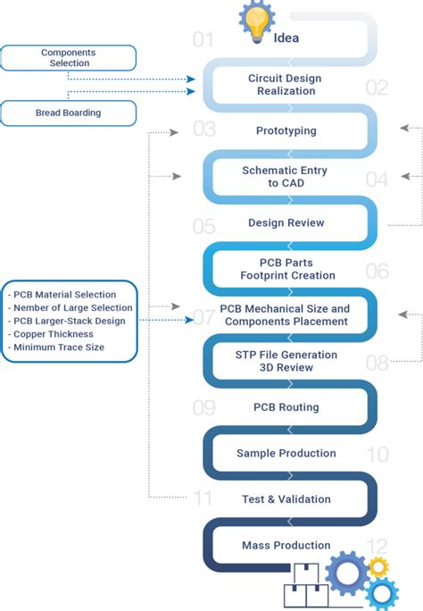
PCB Design for Manufacturing: Key Strategies for High Yield
Key Takeaways
When optimizing designs for PCB manufacturing, understanding core principles ensures your boards meet both performance and production requirements. Start by evaluating component placement—clustering related parts reduces trace lengths and minimizes signal interference, which directly impacts PCB manufacturing cost. Work closely with PCB manufacturing companies during layout reviews to identify potential bottlenecks, such as insufficient clearance between high-voltage components.
Material selection plays a dual role: it affects both durability and yield rates. For instance, choosing FR-4 over specialized substrates might lower upfront expenses but could increase failure risks in high-temperature environments. Always cross-reference your PCB manufacturing business requirements with material datasheets to balance cost and reliability.
Implement DFM validation checks early, focusing on:
| Design Aspect | Traditional Approach | DFM-Optimized Approach |
|---|---|---|
| Trace Width | Fixed for all signals | Adjusted based on current load |
| Drill Hole Sizes | Uniform dimensions | Optimized for tooling standards |
| Solder Mask Clearance | Minimum tolerance | Expanded to prevent bridging |
By prioritizing these strategies, you avoid common pitfalls like overcomplicated layouts or mismatched materials. For deeper insights, review industry-leading DFM guidelines to align your designs with production realities. Remember, seamless integration of DFM principles into your workflow not only boosts yield but also strengthens partnerships with PCB manufacturing providers.
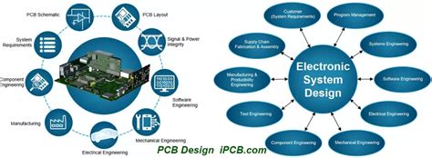
PCB Design for Manufacturing Essentials
When designing printed circuit boards, aligning your layout with PCB manufacturing capabilities is critical to avoid costly revisions. Start by understanding the technical constraints of your chosen PCB manufacturing companies, such as minimum trace widths, drill sizes, and layer alignment tolerances. These parameters directly influence yield rates and PCB manufacturing cost, as tighter tolerances often require specialized equipment or additional quality checks.
Prioritize component placement that balances functionality with assembly efficiency. For example, orienting polarized parts uniformly reduces errors during automated pick-and-place processes. Similarly, maintaining adequate spacing between surface-mount devices (SMDs) prevents solder bridging—a common issue that forces rework and inflates PCB manufacturing business expenses.
Material selection also plays a pivotal role. High-frequency applications may demand low-loss laminates, but these materials can increase PCB manufacturing cost if not optimized. Collaborate early with manufacturers to validate material choices against their production workflows, ensuring thermal and mechanical stability during fabrication.
Finally, integrate DFM validation checks at every stage. Automated tools can flag issues like acid traps or insufficient copper-to-edge clearance, but manual reviews with your manufacturer add an extra layer of assurance. By addressing these essentials upfront, you streamline the transition from design to mass production while safeguarding yield rates and profitability.
Component Placement for DFM Efficiency
Strategic component placement directly impacts PCB manufacturing efficiency and yield. When arranging parts, prioritize spacing between components to avoid assembly conflicts—PCB manufacturing companies often require at least 0.1mm clearance for automated pick-and-place machines. Orient similar components in the same direction to minimize soldering defects, and group related circuits to reduce trace lengths, which lowers signal interference risks.
Tip: Always consult your PCB manufacturing business partner early to align placement rules with their equipment capabilities. This prevents costly redesigns and ensures compatibility with their production workflows.
Avoid placing heat-sensitive parts near high-power components, as thermal mismatches can lead to premature failures. Use symmetrical layouts for balanced copper distribution, which improves warpage resistance during reflow soldering. Additionally, standardize component footprints to reduce PCB manufacturing cost—non-standard sizes may require custom tooling or manual adjustments.
For mixed-technology boards, separate surface-mount (SMD) and through-hole components into distinct zones. This simplifies assembly steps and reduces the likelihood of solder bridging. Finally, verify that critical components like connectors or debug ports are accessible for testing—a step often overlooked until PCB manufacturing issues arise. By optimizing placement for manufacturability, you create designs that transition smoothly from prototyping to mass production.
Material Selection Impact on PCB Yield
Your choice of materials directly influences both the performance and manufacturability of your PCB. PCB manufacturing companies prioritize substrates, laminates, and finishes that balance electrical performance with production feasibility. For instance, selecting a low-Tg (glass transition temperature) material for high-temperature applications risks warping during soldering, leading to yield losses. Conversely, opting for high-quality FR-4 with adequate thermal stability minimizes defects like delamination, ensuring smoother assembly.
Cost considerations also play a role—premium materials may reduce PCB manufacturing cost long-term by avoiding rework, but over-specifying can inflate initial expenses. Collaborate with your fabricator to align material properties with design requirements: high-speed designs demand low-loss dielectrics, while rigid-flex boards need flexible substrates. Additionally, finishes like ENIG (Electroless Nickel Immersion Gold) enhance solderability but add complexity to the PCB manufacturing business process.
Always validate material compatibility with your PCB manufacturing partner early in the design phase. This prevents mismatches in thermal expansion coefficients or chemical resistance, which could trigger failures during testing. By balancing performance, cost, and process compatibility, you ensure materials contribute to—not compromise—yield targets.
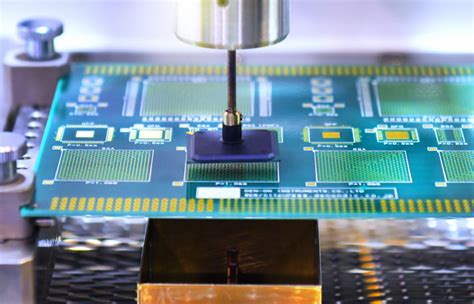
DFM Validation Checks for Quality Assurance
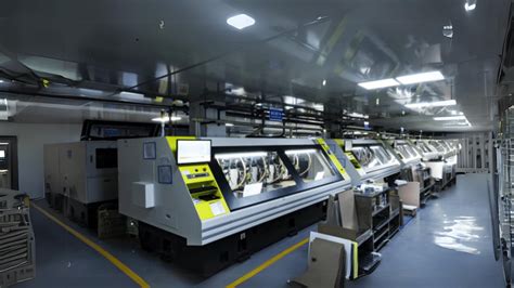
When implementing PCB manufacturing best practices, thorough design validation ensures your board meets production requirements while minimizing errors. Start by running automated DFM checks to verify trace widths, spacing, and annular ring compliance—critical factors that PCB manufacturing companies scrutinize to avoid fabrication delays. Cross-reference your design against the manufacturer’s capabilities, such as minimum drill sizes or layer alignment tolerances, to prevent mismatches that inflate PCB manufacturing cost.
Next, validate thermal management features like copper balancing and via placement, which directly impact solder joint reliability during assembly. Use simulation tools to detect potential warping or stress points, especially when working with high-density designs. Material compatibility checks are equally vital—ensure substrates and finishes align with your PCB manufacturing business environment (e.g., high-temperature or humid conditions).
Collaborate early with your fabrication partner to review stack-up configurations and impedance control requirements. Many PCB manufacturing companies offer pre-production audits, flagging issues like insufficient clearance for automated optical inspection (AOI). By prioritizing these validation steps, you reduce rework risks, streamline timelines, and maintain consistency across batches—key drivers for achieving high yields without compromising quality.
Cost Reduction Through DFM Best Practices
Adopting Design for Manufacturing (DFM) principles directly impacts your ability to lower PCB manufacturing cost while maintaining quality. By prioritizing component placement that aligns with assembly workflows, you reduce the risk of errors during fabrication. For example, spacing high-density components evenly minimizes solder bridging, which prevents costly rework. Collaborating early with PCB manufacturing companies ensures your design adheres to their equipment capabilities, avoiding delays from last-minute adjustments.
Material selection also plays a critical role. Opting for standardized laminate materials instead of custom substrates cuts PCB manufacturing business expenses without compromising performance. Additionally, using panelization techniques maximizes board yield per panel, reducing material waste. Implementing automated DFM validation checks—like testing for minimum trace widths or drill hole alignment—catches issues before production, saving time and resources.
Finally, streamlining documentation (e.g., clear layer stackup notes) helps PCB manufacturing teams execute designs accurately. Small optimizations, such as avoiding non-standard via sizes, add up to significant savings. Remember: every design choice that simplifies assembly translates to lower costs and higher reliability in volume production.
High-Yield PCB Design Core Principles
To achieve consistent PCB manufacturing success, your design must align with the core principles that bridge engineering intent and production realities. Start by prioritizing design symmetry and thermal management—uneven copper distribution or inadequate heat dissipation often lead to warping during assembly, increasing PCB manufacturing cost and delays. Collaborate early with PCB manufacturing companies to understand their equipment tolerances; this ensures features like drill hole sizes and trace widths fall within their capabilities, minimizing rework.
A critical yet overlooked principle is design standardization. Using common component footprints and avoiding exotic materials reduces variability, which is vital for scaling production in a PCB manufacturing business. For example, sticking to standard FR-4 substrates unless high-frequency demands require alternatives keeps costs predictable. Additionally, implement DFM-driven spacing rules—crowded component placement might save space but risks solder bridging, especially in high-density designs.
Finally, integrate DFM validation checks at every stage. Automated tools can flag issues like acid traps or insufficient annular rings before prototypes are sent to fabrication. By embedding these principles, you create a feedback loop between design and manufacturing, ensuring higher yield rates and smoother transitions from concept to mass production.
Avoiding Common DFM Pitfalls in Layouts
Even with careful planning, overlooking PCB manufacturing requirements can lead to costly redesigns or production delays. One frequent mistake is ignoring component-to-edge clearance, which risks damage during panelization. To prevent this, maintain a minimum 3mm margin from board edges, especially for components like connectors or heatsinks. Another pitfall involves improper trace width/spacing for high-current paths—narrow traces may overheat, while insufficient spacing can cause short circuits during etching.
Misjudging PCB manufacturing cost drivers often stems from overly complex layer stacks or unnecessary via-in-pad designs. Simplify layouts by prioritizing standard materials and avoiding exotic finishes unless absolutely necessary. Additionally, failing to account for thermal management in dense layouts can warp boards during reflow soldering, forcing PCB manufacturing companies to reject batches. Always validate copper balancing and use thermal relief pads for high-mass connections.
Lastly, neglecting DFM validation checks before finalizing files is a critical error. Tools like automated DFM analyzers flag issues like acid traps or drill alignment errors, but manual reviews remain essential. Collaborate early with your PCB manufacturing business partner to align on their capabilities—this ensures your design adheres to their process tolerances, minimizing yield losses and last-minute adjustments. By addressing these pitfalls proactively, you streamline production and avoid the hidden costs of rework.
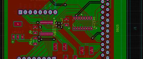
Integrating DFM in PCB Layout Tools
Modern PCB manufacturing demands seamless collaboration between design and production, which is why integrating design for manufacturing (DFM) checks directly into your layout tools is critical. By embedding automated DFM validations—such as minimum trace width checks, component spacing rules, and drill-to-copper clearances—you can identify potential issues before sending files to PCB manufacturing companies. This proactive approach reduces iterative revisions, slashing PCB manufacturing cost and accelerating time-to-market.
Advanced tools now simulate real-world production constraints, like panelization efficiency or material warpage risks, allowing you to optimize designs for specific PCB manufacturing business requirements. For example, setting up rules for solder mask expansion or via tenting within the software ensures compliance with your manufacturer’s capabilities. Additionally, tools that generate manufacturing-ready outputs (Gerber files, drill charts, and assembly drawings) with built-in error reporting minimize miscommunication.
To maximize value, configure your layout software to align with your manufacturer’s DFM guidelines. This includes setting layer stack-ups that match their material inventories or defining fiducial markers for precise assembly. By bridging the gap between design intent and production reality, you ensure smoother transitions from prototype to mass production while maintaining high yield rates.
Conclusion
By prioritizing PCB manufacturing considerations early in your design process, you create a foundation for seamless production and consistent quality. Partnering with experienced PCB manufacturing companies ensures access to industry-specific insights, helping you avoid costly redesigns and delays. Remember that every design choice—from component spacing to material thickness—directly impacts PCB manufacturing cost structures and the scalability of your PCB manufacturing business.
Adopting design validation tools and prototyping workflows allows you to identify potential issues before they escalate, preserving both time and resources. While balancing performance goals with manufacturability might seem challenging, aligning your design decisions with industry standards simplifies collaboration with fabrication teams. Ultimately, a proactive approach to DFM not only elevates yield rates but also strengthens your product’s reliability in competitive markets—proving that smart design is inseparable from efficient production.
Frequently Asked Questions
How does DFM affect pcb manufacturing cost?
By implementing design for manufacturing principles early, you reduce rework and material waste. Proper component spacing and standardized footprints help pcb manufacturing companies avoid costly redesigns, directly lowering your production expenses.
What should you prioritize when selecting pcb manufacturing companies?
Look for partners with dfm validation tools and expertise in your industry. Their ability to flag issues like inadequate copper balancing or improper via sizing ensures smoother transitions from design to pcb manufacturing business operations.
Can component placement impact pcb manufacturing yield?
Yes. Overcrowded components or irregular orientations increase assembly errors. Aligning parts to match automated pick-and-place workflows minimizes defects, boosting yield for high-volume pcb manufacturing runs.
Why are dfm validation checks critical for cost control?
Automated checks identify issues like acid traps or insufficient annular rings before production. Fixing these during design avoids delays and extra charges from pcb manufacturing companies, keeping projects within budget.
How does material selection influence pcb manufacturing business outcomes?
Choosing substrates compatible with standard fabrication processes (e.g., FR-4) reduces lead times. Specialty materials may require custom tooling, escalating pcb manufacturing cost and complicating supplier coordination.
Ready to Streamline Your PCB Production?
For tailored pcb manufacturing solutions that align with DFM best practices, please click here to connect with experts who optimize designs for yield and cost efficiency.


