PCB Design Post-Processing Overview: A Comprehensive Guide
Introduction to PCB Post-Processing
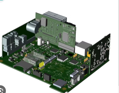
Printed Circuit Board (PCB) design is a complex, multi-stage process that doesn’t end with the completion of the schematic and layout. The post-processing phase represents a critical bridge between design completion and manufacturing readiness, ensuring that the digital design can be accurately translated into a physical product. This often-overlooked stage encompasses numerous essential tasks that verify design integrity, optimize manufacturability, and prepare all necessary documentation for fabrication and assembly.
Post-processing accounts for approximately 20-30% of the total design time in professional PCB development, yet many designers underestimate its importance. Proper post-processing can mean the difference between a smoothly manufactured board and one that requires multiple revisions, delaying time-to-market and increasing development costs. This article provides a comprehensive overview of PCB design post-processing, examining its key components, best practices, and emerging trends in the industry.
Design Rule Verification and Validation
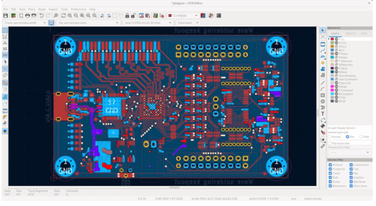
Design Rule Check (DRC)
The cornerstone of PCB post-processing is the Design Rule Check, a systematic verification that the layout complies with all specified design constraints. Modern EDA (Electronic Design Automation) tools perform hundreds of checks in this phase, including:
- Clearance violations: Ensuring adequate spacing between traces, pads, and other copper features
- Width violations: Verifying that trace widths meet minimum requirements for current carrying capacity
- Annular ring checks: Confirming sufficient copper around drilled holes
- Silkscreen overlap: Preventing text or markings from interfering with soldering areas
- Copper pour issues: Identifying islands, sharp angles, or insufficient connections to ground planes
Electrical Rule Check (ERC)
While DRC focuses on physical constraints, ERC examines the electrical integrity of the design:
- Unconnected nets: Identifying floating pins or incomplete connections
- Short circuits: Detecting unintended connections between nets
- Power plane continuity: Ensuring proper distribution of power throughout the board
- Signal integrity basics: Checking for obvious impedance mismatches or termination issues
Manufacturing Rule Check (MRC)
MRC extends beyond generic design rules to address specific capabilities and limitations of the target fabrication facility:
- Minimum drill size: Verifying hole sizes against manufacturer’s drilling capabilities
- Copper-to-edge clearance: Ensuring adequate spacing from board edges
- Solder mask expansion: Confirming proper coverage of pads
- Impedance control: Checking that controlled impedance traces meet specified tolerances
Documentation Preparation
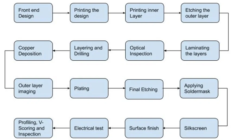
Gerber File Generation
Gerber files remain the industry standard for conveying PCB layer information to manufacturers. Key considerations include:
- File format selection: RS-274X (Extended Gerber) is most commonly used
- Layer mapping: Clearly associating each file with its corresponding board layer
- Aperture definitions: Properly defining all shapes and line widths used in the design
- Inclusion of all layers: Not just copper layers, but also solder mask, silkscreen, paste masks, and drill drawings
Drill File Preparation
Accurate drill data is essential for proper hole creation:
- File formats: Excellon is the most widely accepted standard
- Tool sizing: Listing all required drill bit sizes
- Plated vs. non-plated holes: Clearly distinguishing between hole types
- Stackup information: Providing details for blind/buried vias in multilayer boards
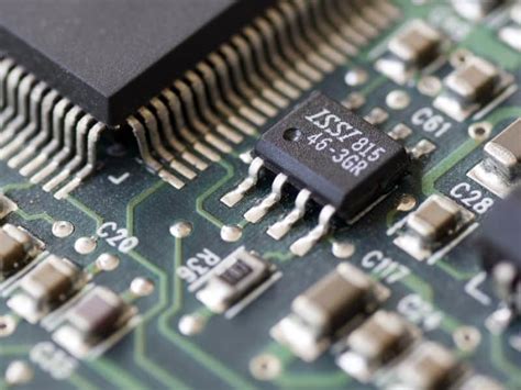
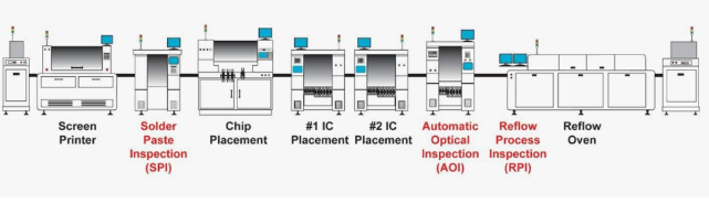
Assembly Documentation
Supporting documents for the assembly process include:
- Pick-and-place files: Component centroid data for automated assembly machines
- Bill of Materials (BOM): Complete parts list with reference designators, values, and manufacturer part numbers
- Assembly drawings: Diagrams showing component placement and orientation
- Special instructions: Noting any unusual assembly requirements or handling considerations
Manufacturing Optimization
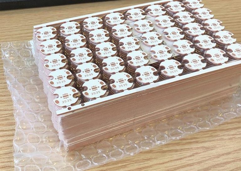
Panelization Considerations
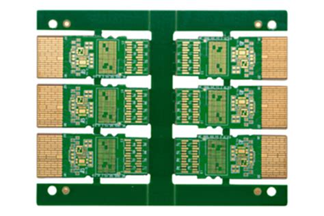
For efficient production, individual PCBs are often combined into panels:
- Array configuration: Determining optimal board arrangement
- Breakaway methods: Designing tabs, v-grooves, or perforations for depanelization
- Fiducial markers: Adding optical reference points for assembly equipment
- Test coupon inclusion: Incorporating test structures for process verification
Copper Balancing
Preventing board warpage through proper copper distribution:
- Layer symmetry: Maintaining similar copper densities on opposite layers
- Thieving patterns: Adding non-functional copper to balance density
- Thermal relief considerations: Ensuring proper heat distribution during soldering
Surface Finish Specification
Selecting the appropriate surface treatment:
- HASL (Hot Air Solder Leveling): Traditional, cost-effective finish
- ENIG (Electroless Nickel Immersion Gold): Flat surface ideal for fine-pitch components
- OSP (Organic Solderability Preservative): Environmentally friendly option
- Immersion Silver/Tin: Alternatives with specific advantages for certain applications
Quality Assurance Measures
Design for Manufacturability (DFM) Analysis
Proactively identifying potential production issues:
- Minimum feature size verification: Confirming compliance with fabrication capabilities
- Solder joint evaluation: Assessing pad sizes for reliable connections
- Component spacing analysis: Ensuring adequate clearance for assembly tools
- Thermal stress points: Identifying areas prone to thermal-induced failures
Design for Testability (DFT) Implementation
Facilitating post-assembly testing:
- Test point placement: Adding accessible points for probe contact
- Boundary scan support: Incorporating JTAG-compatible structures
- Functional test considerations: Designing for bed-of-nails or flying probe testing
- Diagnostic accessibility: Ensuring critical signals can be measured
Version Control and Archiving
Maintaining design integrity through proper documentation:
- Revision tracking: Clearly marking all design iterations
- Package completeness: Including all relevant files in the release package
- Archive formats: Using non-proprietary formats for long-term storage
- Design notes: Documenting critical decisions and unusual features
Advanced Post-Processing Techniques
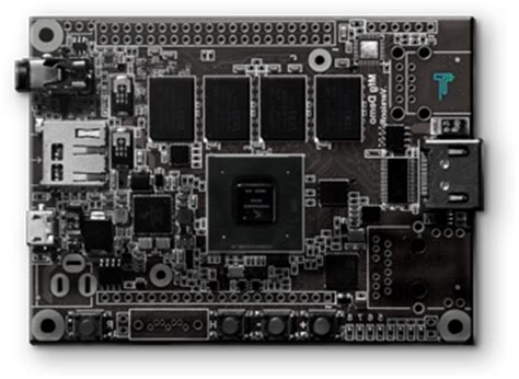
3D Model Export and Verification
Modern PCB design often includes mechanical integration:
- STEP file generation: Creating accurate 3D representations of the PCB
- Mechanical interference checking: Verifying component clearance in the enclosure
- Thermal simulation preparation: Exporting models for CFD analysis
- Assembly animation: Creating visuals for manufacturing instructions
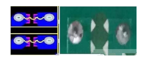
Signal Integrity Verification
While primarily a pre-layout activity, some checks extend to post-processing:
- Cross-section analysis: Verifying impedance calculations against actual stackup
- Return path verification: Checking reference plane continuity
- Power delivery network (PDN) analysis: Assessing decoupling strategy effectiveness
Supply Chain Preparation
Linking design to procurement and manufacturing:
- Component availability checking: Verifying parts against distributor inventories
- Alternate part identification: Specifying acceptable substitutes
- Lead time analysis: Identifying potential bottlenecks in component sourcing
- Cost optimization: Evaluating alternative materials or configurations
Emerging Trends in PCB Post-Processing
AI-Assisted Verification
Artificial intelligence is transforming post-processing through:
- Automated error detection: Machine learning algorithms identifying potential issues
- Manufacturing yield prediction: Estimating production success rates based on design characteristics
- Self-healing designs: Automatic correction of common violations
- Process-aware optimization: Tuning designs for specific factory capabilities
Cloud-Based Collaboration
Modern workflows leverage cloud technology for:
- Real-time design reviews: Simultaneous multi-party verification
- Manufacturer feedback integration: Direct input from fabrication partners
- Version synchronization: Maintaining consistency across distributed teams
- Automated DFM checks: Cloud-based analysis against manufacturer specs
Digital Twin Integration
Creating virtual representations that extend beyond traditional documentation:
- IoT-ready designs: Incorporating connectivity for smart manufacturing
- Lifetime monitoring: Embedding structures for in-field performance tracking
- Predictive maintenance features: Designing for future diagnostic needs
- Augmented reality support: Creating assets for AR assembly guidance
Conclusion
PCB design post-processing represents the critical final phase where theoretical designs are transformed into manufacturable products. This comprehensive set of verification, optimization, and documentation steps ensures design intent is properly communicated to fabrication and assembly partners while proactively addressing potential production issues. As PCB technology advances with higher densities, faster signals, and more complex materials, the importance of thorough post-processing only increases.
Modern EDA tools continue to automate many post-processing tasks, but human expertise remains essential for interpreting results, making judgment calls, and handling exceptional cases. By investing time in proper post-processing, design teams can significantly reduce respins, improve yields, and accelerate time-to-market—ultimately delivering higher quality products more efficiently.
The future of PCB post-processing lies in tighter integration with manufacturing systems, increased automation through AI, and more sophisticated simulation capabilities that blur the line between design and production. Regardless of technological advancements, the fundamental goal remains unchanged: ensuring that the carefully crafted PCB design can be reliably and cost-effectively translated into physical reality.