PCB design tips for input capacitors of switching power supplies
When designing the PCB of a switching power supply circuit, the layout and routing of the input capacitors are crucial, as they directly affect the performance, efficiency, and EMI performance of the circuit. The following are PCB design tips for input capacitors:
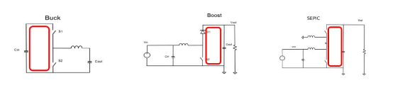
1.Keep as close to the power switch and input terminal as possible
Reason: The main function of the input capacitor is to provide transient current to the switch tube and reduce voltage fluctuations. Placing the input capacitor close to the power switch (MOSFET or IC) and the input pin can minimize the voltage spike caused by parasitic inductance.
Method: Place the input capacitor close to the VIN and GND pins of the Buck controller or power switch.
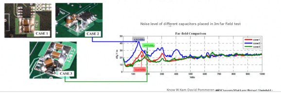
As shown in the figure below, case 1 is close to the chip to prevent it, and the noise radiated by it is detected as the red curve in the figure;
Case 2 is to deliberately stand up the capacitor, and you can see that it has the largest noise, the blue curve;
Case 3 is to bridge the input capacitor between VIN and GND, and the routing distance is the shortest, which is the green curve in the figure, with the smallest noise.
2.Give priority to low ESR and low ESL capacitors
Reason: The input capacitor needs to respond quickly to high-frequency currents. Low ESR (equivalent series resistance) and low ESL (equivalent series inductance) capacitors can filter high-frequency noise more efficiently.
Practice: Use a combination of ceramic capacitors (to filter high-frequency noise) and electrolytic or tantalum capacitors (to provide large capacitance).
3.Reduce the current loop area
Reason: The high-frequency current at the input of the Buck circuit flows between the input capacitor and the power switch. The larger the loop area, the higher the radiated EMI and parasitic inductance.
Practice: Ensure that the path between the ground terminal (GND) of the input capacitor and the ground terminal of the power switch is as short as possible. Try to make the loop between VIN and GND as small as possible.
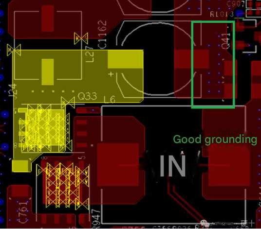
4.Optimize the ground plane connection
Reason: The ground terminal of the input capacitor needs to be directly connected to the ground terminal of the power switch or IC. If the connection path is long or there is current shunting, the ground potential will be unstable.
Practice:
Lay a complete ground plane under the ground terminal of the capacitor.
Use multiple vias to connect the GND pad of the capacitor to the ground plane.
5.Optimize the layout by connecting multiple capacitors in parallel
Reason: A single large-capacity capacitor may not provide sufficiently low ESR and ESL. Connecting multiple small-capacity capacitors in parallel can share high-frequency currents and reduce parasitic parameters.
Practice:
Connect multiple ceramic capacitors in parallel, usually choosing a combination of 10µF, 1µF, and 0.1µF.
Arrange capacitors of different capacities according to frequency requirements: capacitors with high-frequency requirements are closer to switches.
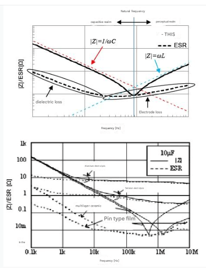
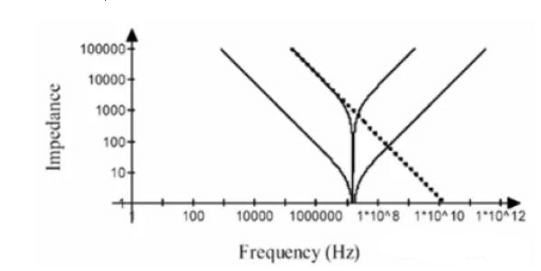
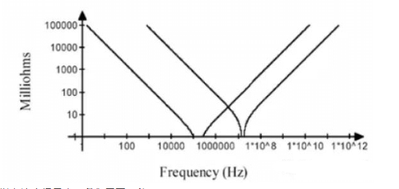
Actual capacitors have parasitic inductance and equivalent series resistance. Since the ESR and ESL of a single capacitor are similar, their impedance characteristics are also similar. The impedance characteristics of a single capacitor and multiple capacitors with the same characteristics in parallel are shown in the figure.
Capacitors with different capacitance values
So in this scenario, we need a:
- 1nF~10uF capacitance, with low precision requirements;
- Due to the large usage (more power pins), the cost is relatively low and the volume is relatively small under the same capacity;
- Capacitors with relatively small ESR and ESL. (The signal frequency that needs to be decoupled is relatively high, and the decoupling effect must be guaranteed)
- Avoid using long traces to connect input capacitors
Reason: Long traces increase parasitic inductance, resulting in increased voltage fluctuations at the input end and possible spike voltages.
Practice: The path between the input capacitor and the controller input pin should be as short and direct as possible, avoiding wiring that is too long or has multiple corners.
8.Check the heat distribution
Reason: The input capacitor is in high-frequency current, which may cause heat due to power consumption.
Practice:
Ensure that there is a good heat dissipation path around the capacitor.
If multiple capacitors are used to share the current, be careful to arrange them evenly to reduce local overheating.
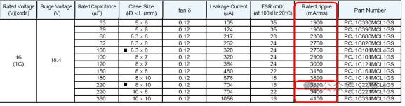
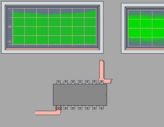
Pay attention to the heat sources around the capacitors, the self-heating of the capacitors, and the maximum effective current value they can withstand in the above figure.
Through the above tips, the PCB design of the input capacitors of the switching power supply circuit can be significantly optimized, improving the stability and efficiency of the system and reducing EMI problems. If more specific schematics or tool support are needed, we can discuss further!